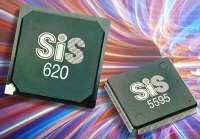
| SiS620/5595

key features
Supports Intel Pentium II CPU Host Bus at 66/100 MHz Front Side Bus
Frequency
- 100/100 and 66/66 MHz Synchronous Host/DRAM clocking configuration
- 100/75 and 66/100 MHz Asynchronous Host/DRAM clocking configuration
- Supports Host Bus operation for integrated 3D VGA Controller
Meets PC99 Requirements
Supports PCI Revision 2.2 Specification
Integrated Super AGP VGA for Hardware 2D/3D Video/Graphics Accelerators
- Supports tightly coupled 64 bits 100MHz host interface to VGA to speed
up GUI performance and the video playback frame rate
- Supports Multiple Adapters and Multiple Monitors
- Flexible design for shared frame or local frame architecture
- Shared System Memory Area 2MB, 4MB and 8MB
- Supports SDRAM and SGRAM local frame buffer and memory size up to 8 MB
- Supports Digital Flat Panel Port for Digital Monitor (LCD Panel)
- Supports DVD H/W Accelerator
Integrated Second Level ( L2 ) Cache Controller
- Write Back Cache Mode with Direct Mapped Cache Organization
- Supports Pipelined Burst SRAM and 256K/512K/1M/2M Bytes Cache Sizes
Integrated DRAM Controller
- Supports up to 3 double sided DIMMs and 8Mbytes to 1.5 Gbytes of main
memory
- Supports Cacheable DRAM Sizes up to 256 MBytes.
- Supports 1M/2M/4M/8M/16M/32M x N for 2-bank or 4-bank SDRAM
- Supports CAS before RAS Refresh, Self Refresh
Provides High Performance PCI Arbiter.
- Supports up to 4 PCI Masters
Integrated Posted Write Buffers and Read Prefetch Buffers to Increase
System Performance
Fast PCI IDE Master/Slave Controller
- Supports IDE PIO Timing Mode 0, 1, 2 ,3 and 4
- Supports Multiword DMA Mode 0, 1, 2 and Ultra DMA 33/66
Supports NAND Tree for Ball Connectivity Testing 576-Balls BGA Package
3.3V Core with mixed 2.5V, 3.3V and 5V I/O CMOS Technology
SiS620/5595 overview
The SiS620 integrates the high performance host bus interface, the DRAM
controller, the IDE controller, the PCI interface, 2D/3D Graphics
accelerator and video playback accelerator. The DRAM controller supports
3-DIMM/6-Bank of 3.3V SDRAM. The maximum memory size supported per bank is
256MB, with a total of 1.5GB system memory. The memory clock frequency can
be operated at up to 100MHz and can be in synchronous or asynchronous modes
with respect to host bus frequency. The supported host/DRAM clock schemes
include: 100/100, 83/83, 75/75, 66/66, 100/75, 100/66, 83/66, 66/83 and
66/100. For power saving, the SDRAM can be put into suspend mode.
The IDE controller is ATA-3 compliant, supporting PIO mode 0/1/2/3/4, DMA
multiword 0/1/2 and Ultra DMA 33/66 operations. The two IDE channels are
fully independent with dedicated 16 double-word FIFO built-in.The PCI
interface is PCI2.2 compliant and supports up to 4 PCI masters. The built-in
PCI arbiter uses rotating priority arbitration scheme with guaranteed
minimum access time for PCI masters, providing fair access as well as low
latency for each PCI masters. The integrated 2D accelerator is a 64-bit
BITBLT graphics engine. It supports all 256 raster operations and
DirectDraw. The accelerated primitives include: BLT, Transparent BLT, Color
expansion, Clipping, Multiple scanline, Polylines, Patterns, Trapezoid
Fills. Up to 8MB of frame buffer can be used with linear addressing.
The integrated 3D graphics accelerator is composed of the triangle setup
engine and the rendering engine. The hardware acceleration features can be
enabled by SiS driver under Direct 3D. The supported 3D quality acceleration
include: Gouroud Shading, Z buffer, Alpha buffer, Perspective Correction,
MipMaping, Tri-linear Texture Filtering, Specular Lighting and Dithering.
The integrated graphics accelerator is compatible with AGP1.0 and PCI2.2
configuration. SiS620 provides two options-UMA and Non-UMA modes for display
memory allocation. In UMA mode, the display memory is shared with system
memory. In Non-UMA mode, the display memory can be up to 8MB SDRAM or SGRAM.
In UMA mode operation, the integrated graphics accelerator uses up to 8MB
of system memory as display memory, thereby saving the on-board DRAM cost
for building a PC system. To reduce the performance degradation inherent
from the UMA architecture, SiS620 has included the super-AGP architecture,
which consists of dual 64bits data path. One data path is between VGA and
host bus, the other is between VGA and system memory. Both data paths are
operating at 100MHz and provide 800MB/s bandwidth. The internal arbitration
logic further allows concurrent transactions to take place in different data
paths. As a result, the overall system performance can be maintained at a
reasonable high level while maximum cost-saving is achieved.
In non-UMA mode, on-board SDRAM or SGRAM (up to 8MB) will be used as
display memory. This gives system designers an option to achieve maximum
system performance. The super-AGP architecture provides 800MB/s bandwidth
between VGA and host bus, which is 50% more than the AGP 2X mode (532MB/s).
The display memory interface bus frequency can also be operated at up to
100MHz, with 64-bit or 32-bit data path(the 32-bit data path configuration
gives the designer a low-cost solution). In summary, SiS620 provides
consistent 800MB/s bandwidth among internal module as well as external
memory interfaces, and delivers high performance in 2D and 3D applications.
For flat panel display support, SiS620 provides external LVDS/TMDS
controller interface. This interface shares the pins with display memory
data bus[63:32], therefore, the flat panel function is available only in UMA
mode or in 32-bit non-UMA mode.
The SiS5595 PCI system I/O integrates the PCI-to-ISA bridge, KBC, USB,
RTC, SMBUS, ACPI/APM compatible PMU, system environment monitoring for
thermal, fan, voltage as well as comprehensive PCI audio support including
DDMA, TDMA and SB-Link.
SiS620/5595 pic
Related Information
Key features
Drivers
Sales contact
|