|
History of Intel Graphics card
yjfy |
|
This article is about the history of Intel's graphics and display chips
based on hardware collections. In order to reflect the authority of this
article, the intel graphics cards in the text are mostly representative
engineering samples from myself and Tibetan friends. Thanks to the
computer hardware collection, such rare computer hardware can get rid of
destruction.
This article introduces the history of Intel graphics cards into four
periods.
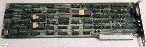
1. 12 years of drifting ( 1977-1988 )
Intel's original graphics card is for VIDEO/GRAPHICS MODULE on Intel
Single Board Computers, a display module with display capabilities.
Although it is only the prototype of the graphics card, it has an
important position in the history of Intel graphics. After Intel
released several display chips, it was used by many manufacturers to
make graphics cards, but Intel still disdain to enter the PC graphics
market, because Intel's business focus at this time is memory and
processor.
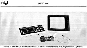
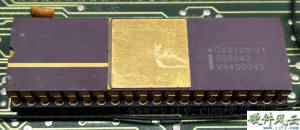
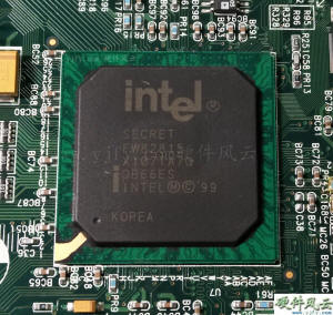
1.1 8275 Chip
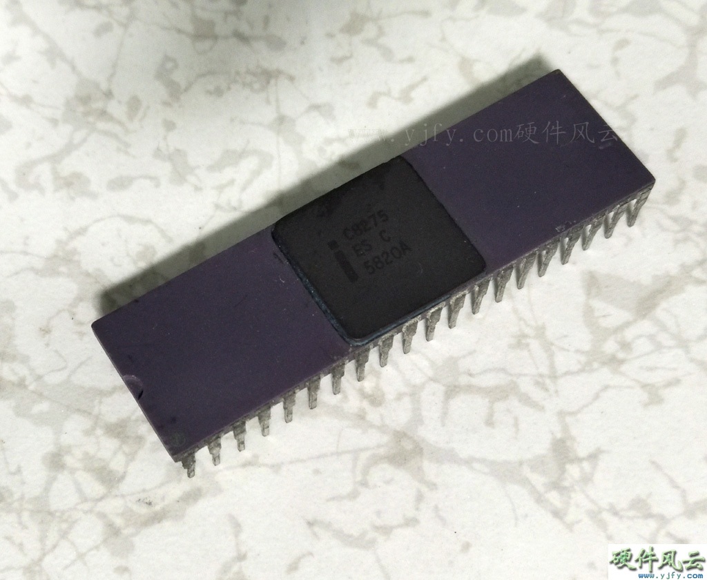
C8275 Engineering sample
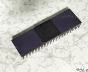
Pictured above is Intel's first display-related chip C8275 CRT
Controller, which is an engineering sample chip with a date of 7735,
indicating that the C8275 chip first appeared in the 35th week of 77
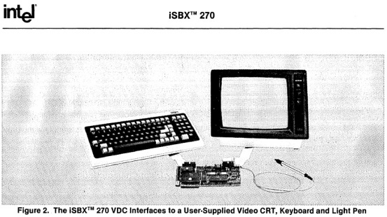
(late mid-August). Used in Intel's iSBX270 VIDEO DISPLAY CONTROLLER
MULTIMODULE Board. The iSBX 270 VDC contains 4K bytes of high speed
static RAM.
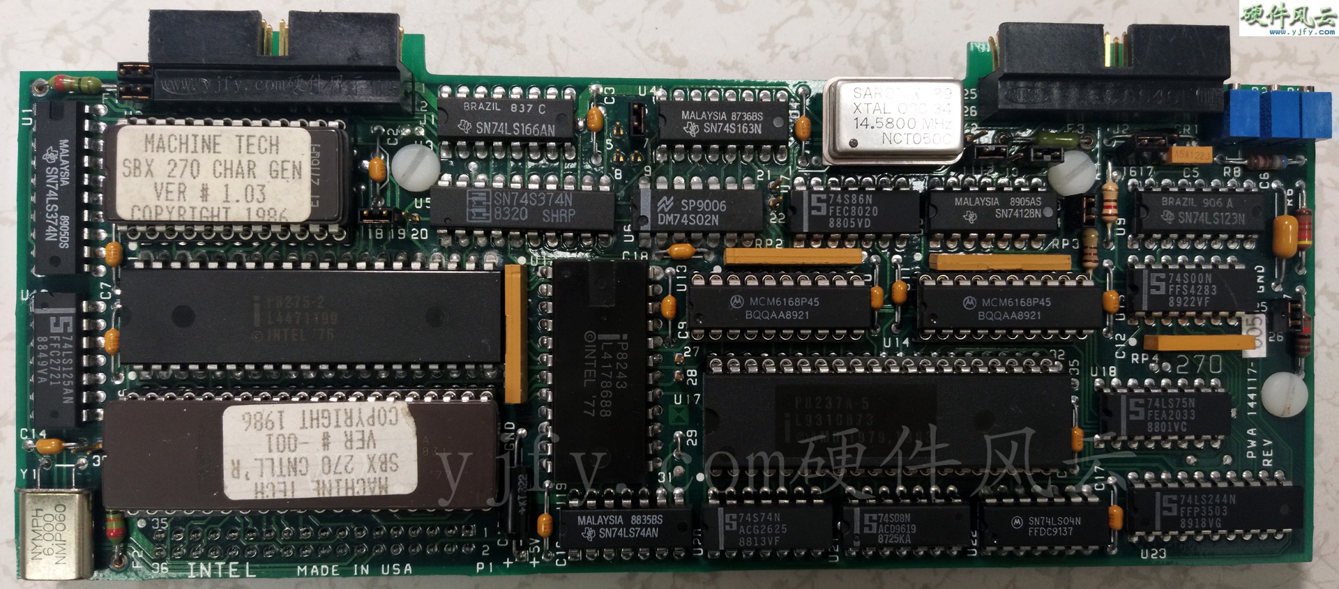
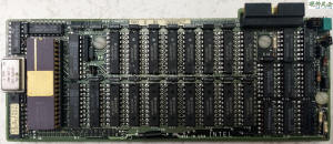
iSBX270

Processor II 2217605132
The iSBX270 was well-known in the past and was also used on the
Processor II 2217605132 Multibus card from non-intel Machine Technology
Inc.
Later, Intel also introduced the 8275 chip upgrade version 8276 chip.It
is small system CRT controller. It is meant to interface CRT raster scan
displays with Intel 8085, 8086, 8088 microprocessors and 8051 single
chip microcomputer. It has 4 types of cursor control, programmable
screen and character format, 6 independent visual field attributes. It
contains all necessary counters,buffers, raster timing circuitry and
video control, etc.
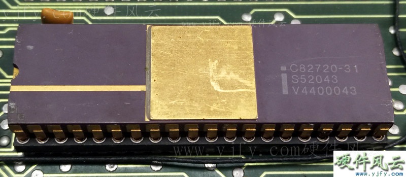
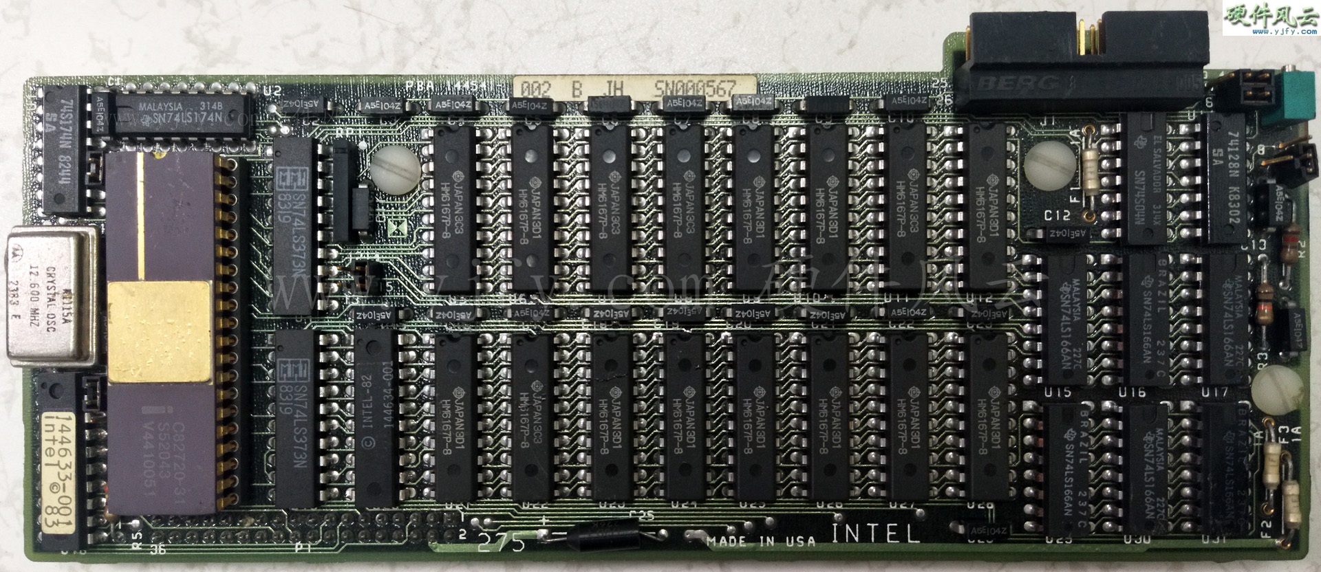
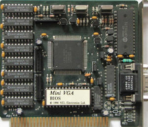
1.2 82720 Chip
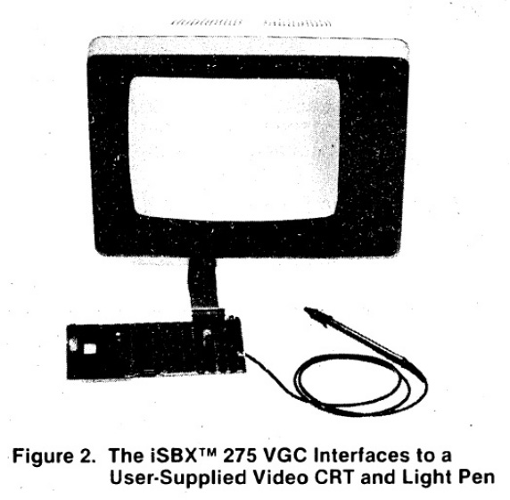
Launched in 1982 iSBX275 VIDEO GRAPHICS CONTROLLER MULTIMODULE
Board.The iSBX275 VGC contains 32K bytes of high speed display memory.
iSBX275
Some
people think that the iSBX275 is INTEL's first graphics card. Perhaps
this view is from Intel Corporation annual report 1982:“The 82720
Graphics Display Controller enhances both development and execution
speed of color graphics applications, making high quality color graphics
affordable for general purpose business systems. It is the first in
Intel's family of high-performance CRT controllers.”
In 1981, after entering the PC era, intel did not immediately
intervene in the field of PC graphics. Because Intel's main business is
CPU, and Intel Single Board Computers an important task is to test and
evaluate the CPU.
iSBC
86
NEC started the 7220 project in 1979 and released μPD7220 in 1981.NEC’s
µPD7220 was the first integrated graphics controller chip.The chip
aincorporated all the CRT control functions (known as the CRTC) as well
as graphics primitives for arcs, lines, circles and special
characters.At that time, the μPD7220 was very advanced. Intel was used
to improve the display performance of the system. The μPD7220 directly
cloned NEC was 82720.Announced in 1982, it was the first of what would
become a long line of Intel graphics processing units.

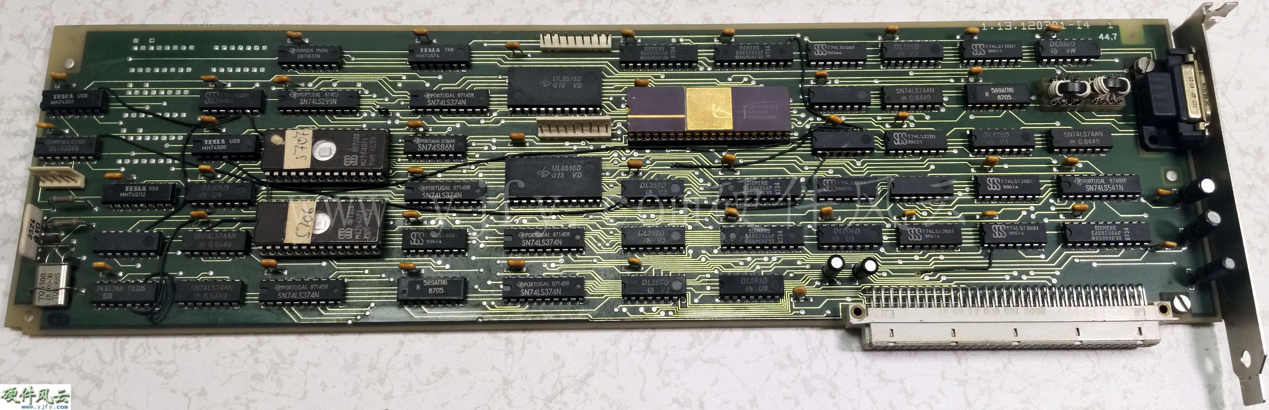
The 82720
chip is also used in computer graphics cards, 1.13.120301-I4 graphics
card of Robotron EC-1834.
1.13.120301-I4
1.3 82730 Chip
In 1982, Intel introduced the 82730 chip. The Intel System
Development Kit SDK-186 has 82730 chips. 82730 chip is Text coprocessor:Supports high-quality text displays with proportional
spacing, subscript/superscript, character attributes, etc.Supports
high-quality graphics with manipulation and display of bitmap strings.
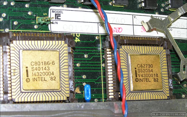
The picture above shows the C82730 chip used on the REGNECENTRALEN
RC759 PICCOLINE computer. Intel 80186 (or 80186) is Intel's embedded
market for industrial control/communication. It is very rare for PCs
like this, let alone the 82730 chip application.
C82730
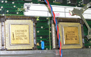
REGNECENTRALEN RC759 PICCOLINE
(Source from http://www.old-computers.com collectibles)
1.4 82716 Chip
The 82716 chip appeared in 1984.It is a video storage and display
device. It is a low cost, highly integrated video controller. It
displays texts and graphics. It can manage upto 16 display objects on
the screen at any time. It can select upto 16 colours from a range of
4096.It contains on-chip DRAM controller and on-chip D/A converters. It
can support upto 512 KB of display memory. It is compatible with 8.and
16-bit microprocessors and microcontrollers.
I have not seen the graphics card of the 82716 chip, maybe it is used on
professional equipment.
N82716
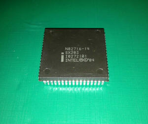
(Image courtesy of hitech-components from eBay.com)
1.5 82786 Chip
In 1986, Intel introduced the 82786 chip, the first discrete graphics
coprocessor. The 82786 integrates a graphics processor, a display
processor with a CRT controller, a bus interface unit (BIU), and its
DRAM/VRAM controller. Support 4 MB of DRAM / VRAM memory. Supporting up
to 256 colors, systems with multiple 82786 designs can support virtually
unlimited colors and resolutions.
The 82786 chip is used in the iSBX279 of the Intel Single Board
Computers system.
iSBX279
(from http://www.intel-vintage.info)
The A82786 chip has also been produced by many manufacturers, such as
the NUMBER NINE Pepper graphics card of the ISA interface of the PC
system.
NUMBER NINE
Pepper
It is a CHMOS graphics coprocessor. It is compatible with all Intel
microprocesors. It can support multiple graphics applications from
multiple graphics bitmaps. It has high speed character drawing, fast
polygon and line drawing capability. It can support upto 200 MHZ CRTs.
It provides upto 256 simultaneous colours. It contains DRAM/VRAM
controller for graphics memory upto 4 MB. It contains shift registers
and DMA channels. It is a powerful device developed for microcomputer
applications including PCs, engineering workstations, terminals and
laser printers. High integration makes it cost-effective.
1.6 i750 Chip
Intel's i750 chip consists of i750PA (82750PA pixel processor) and
i750DA (82750DA display processor). The technical parameters are:The
82750PA is a 25 MHz wide instruction processor that generates and
manipulates pixels. When paired with its companion chip, the 82750DA,
and used to implement a DVI Technology video subsystem, the 82750PA
provides real time (30 images/sec) pixel processing, real time video
compression, interactive motion video playback and real time video
effects.
Intel's i750PA/DA chip was made in December 1986. The i750 design is
so advanced that it is only viewed by DVI Technology (Digital Video
Interactive), with the DVI (Digital Video Interactive) concept (all
digital sound, text, graphics processing system, can support a variety
of multimedia information sources and information formats.) Developed a
DVI Pro 750 graphics card. Intel is optimistic about this concept and is
more optimistic about the development prospects of digital multimedia
technology. On November 14, 1988, it acquired the pioneer of digital
media DVI Technology.
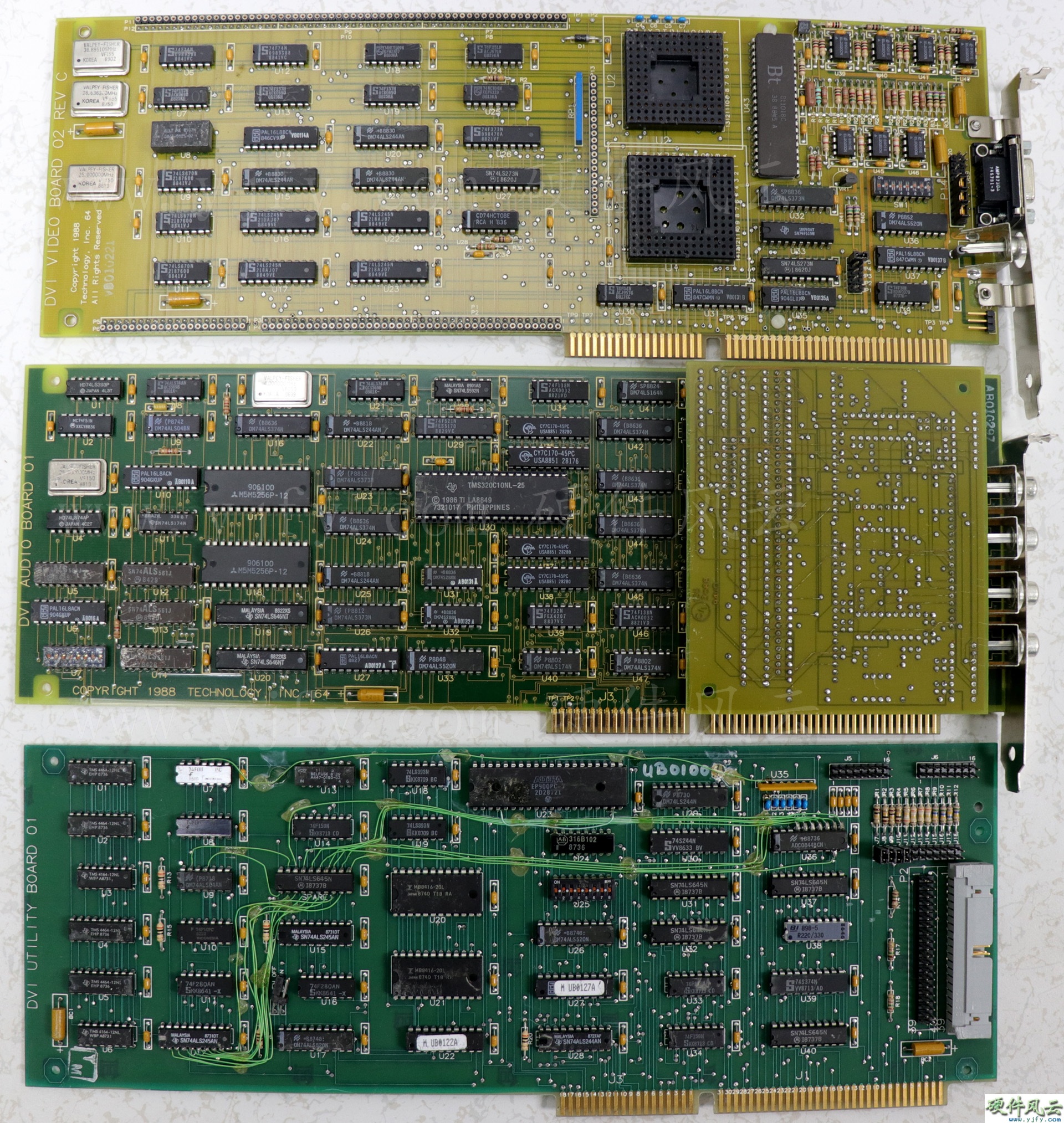
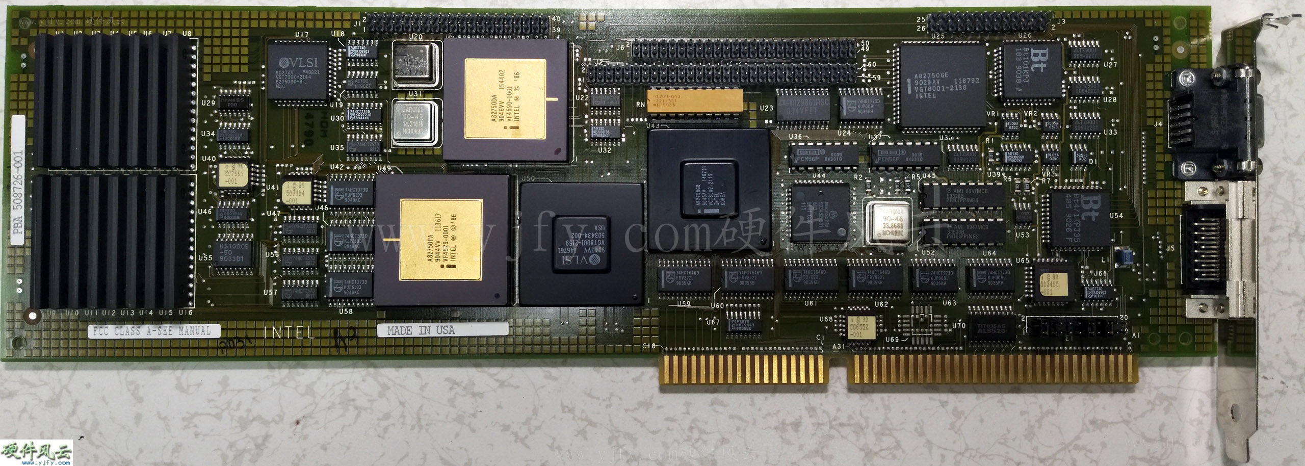
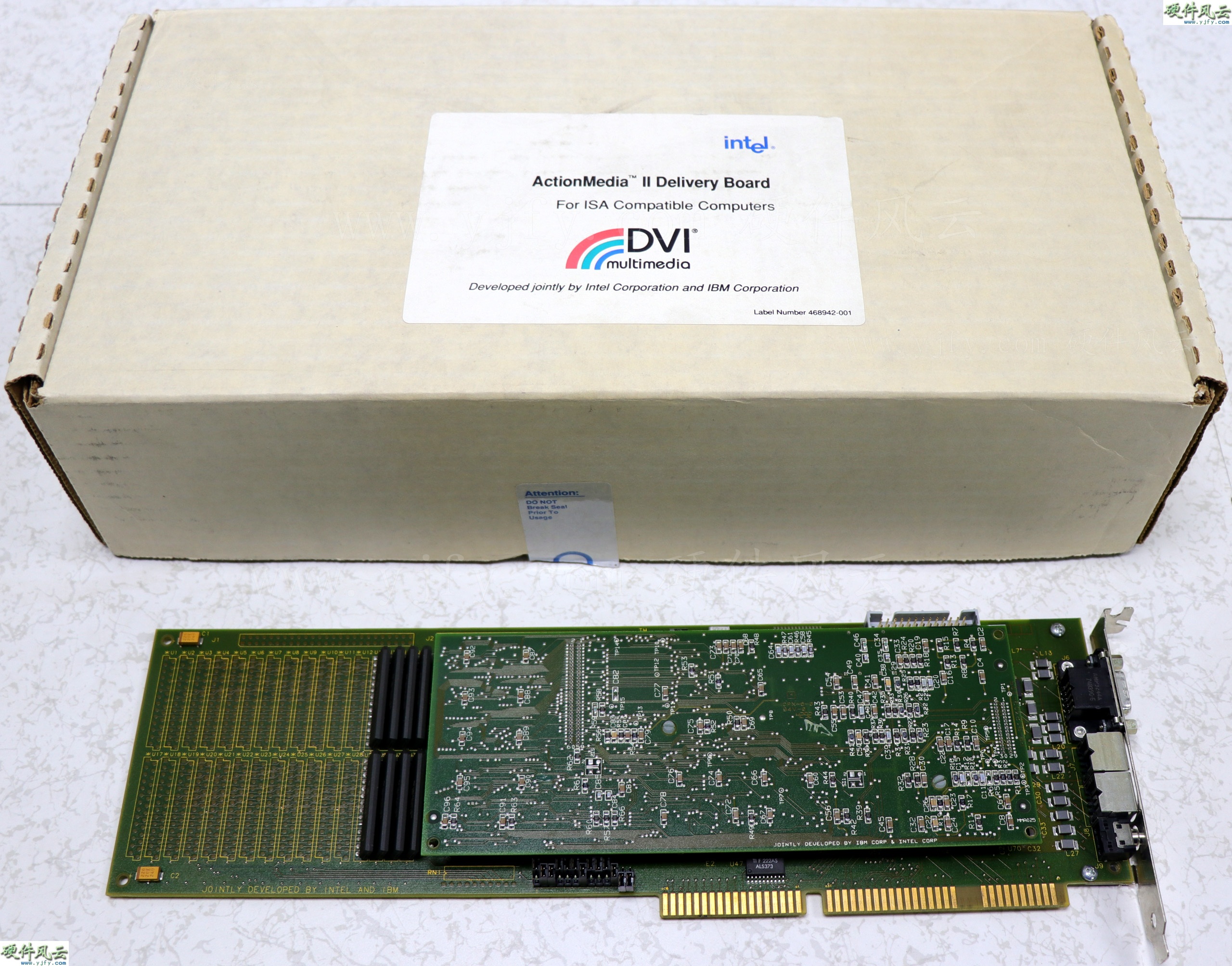
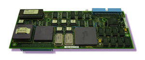
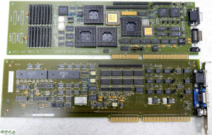
The picture below shows the main card of the DVI/intel Pro 750
graphics card. The full set has 3 ISA interface boards and 3 daughter
cards.
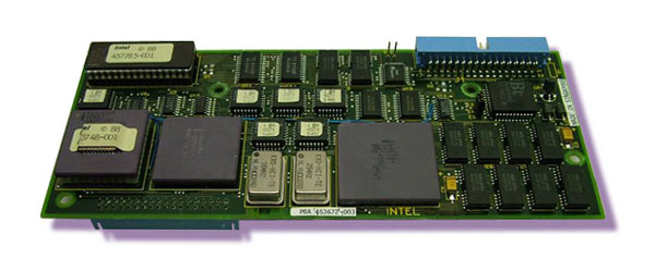
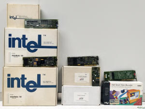
Pro 750 Engineering sample
The full DVI/intel Pro 750 is at least 3 boards (Video, Audio,
Utility/CD-ROM) and 3 daughter cards(Video Digitizer, Audio Digitizer,
4MB of VRAM memory) “actually three boards (Video, Audio,
Utility/CD-ROM) in three slots (with possible overhang), plus add-in
piggyback modules for a Video Digitizer, Audio Digitizer, and 2 GB of
VRAM memory.” DVI/intel Pro 750.
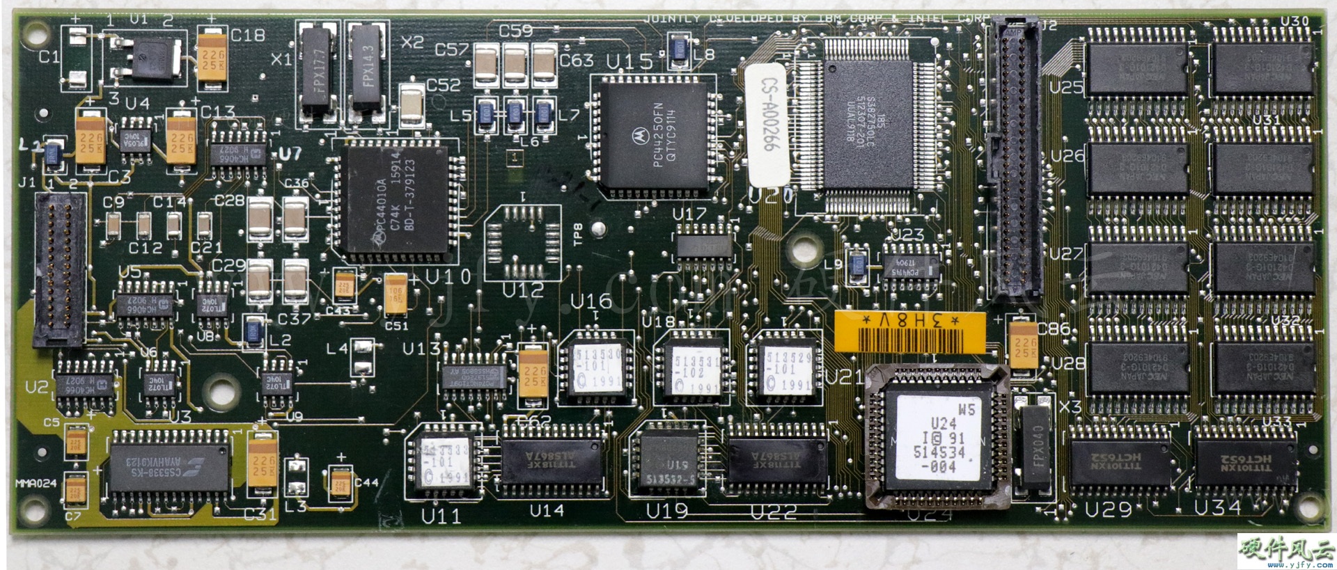
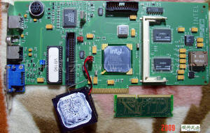
In my collection of DVI/intel Pro 750 engineering samples, the date is
the Utility card and the PCB date is 8809. Explain that in March of the
same year, DVI has produced the Pro 750 prototype card, but it was not
officially released by INTEL and Microsoft until July 21, 1989.
1.7 KAMA 芯片
See only the Vlask collection of Intel Kama graphics cards from http://www.vgamuseum.info.
Kama
Failed to find information about the KAMA chip. However, it is judged
from the shape and label of the chip that it is associated with the
i750DB chip.
The KAMA chip is labeled as:
KAMA SX094
K8909B-25 V1.6
I9082207
INTEL m © '87
Can be seen:
1.The "-25" in K8909B-25 has a meaning of 25MHz. It can be seen that
it is also a display processor.
2. I9082207 shows that the production date is 08th week of the year
89.
3, INTEL m © '87, indicating the development of 87 years, i750DA,
PGA pin structure developed later than 86 years. In 1989, the i750DB
chip was upgraded to the PQFP patch structure.
It can be seen that the KAMA chip is based on the i750DB chip and is
improved using the DRAM memory display chip.Also similar to the 82706
chip.
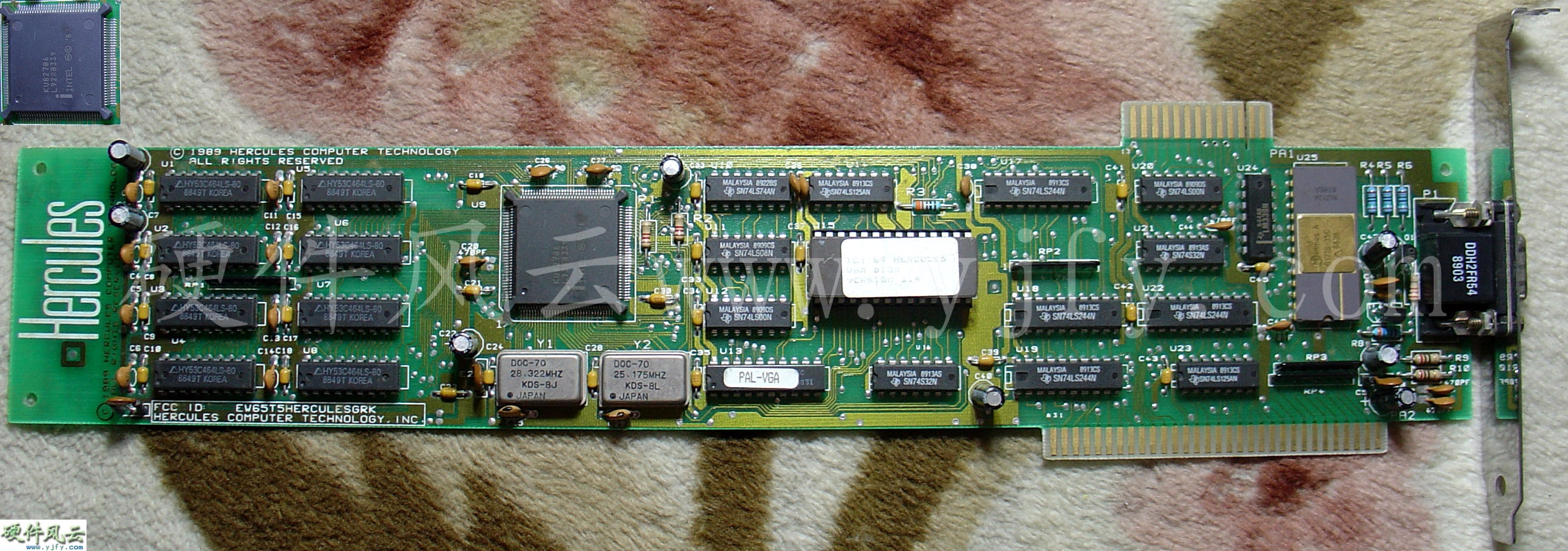
1.8 82706 Chip
Intel launched 82706 in 1988. It is an Intel video graphics array(VGA)compatible display controller for IBM PC/XT/AT and PS/. All
video monitors developed for IBM PS/2 system are provided with VGA
controller. The 82706 can support 256 KB video memory. It is designed to
be compatible with 80286 and 80386 and other microprocessors. It has EGA/CGA/MDA
BIOS compatibility. It acts as CRT controller and video memory
controller.
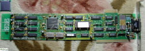
Hercules VGA card is made by Hercules with this chip.
Hercules VGA
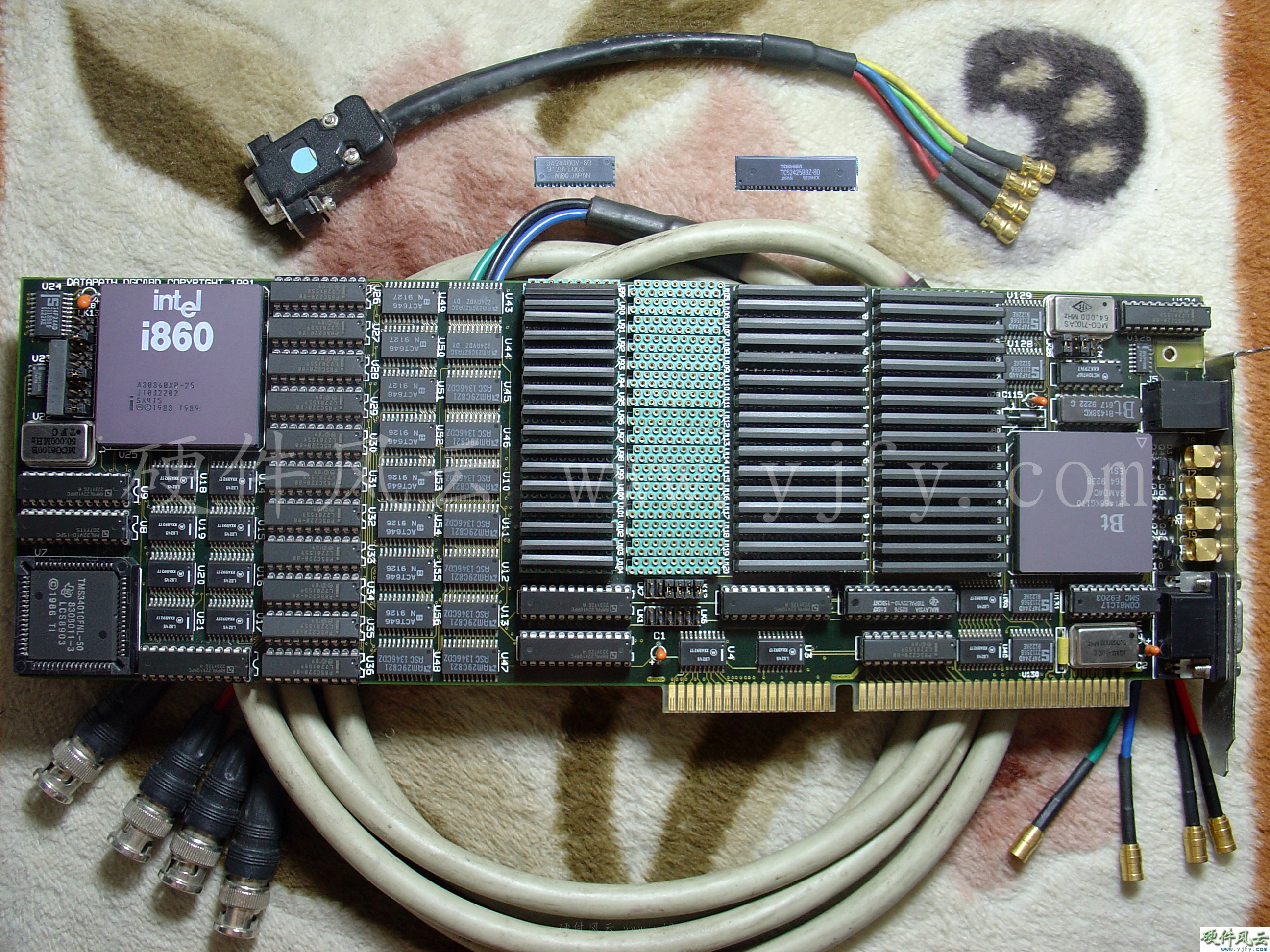
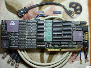
1.9 i860 Chip
On February 27, 1989, Intel launched the i860. At that time, i860 was
the most advanced 64 bit microprocessor, adopting RISC design
technology, which was a general-purpose high-performance microprocessor.
It integrates the core components of integer RISC, floating-point
processing, page memory management, instruction cache, data cache and 3D
image processing into a VLSI microprocessor. In short, i860 is like core
I3 / i5 in 20 years. Advanced design leads to its high price, and its
graphics card only appears in the high-end professional field.
DATAPATH DGC0BD
|
|
2. The first fledgling (1989-1996)
I introduced the i750 chip in the previous section. After Intel
acquired DVI, the DVI Pro750 graphics card was renamed Intel Pro750.
However, INTEL is very dissatisfied with the design of the PRO 750
graphics card, and re-developed the ACTIONMEDIA series of graphics
cards, thus officially entering the field of PC graphics.
The Intel i750 graphics card project lasted for 6 years and it is
obvious that it is doing its best. In order to expand the impact, even
with the PC giant IBM. Unfortunately, in the era of the heroes, Intel's
efforts still have no breakthroughs, gradually disappeared. So senior
hardware enthusiasts only think that Intel's first graphics card starts
with the i740 chip...
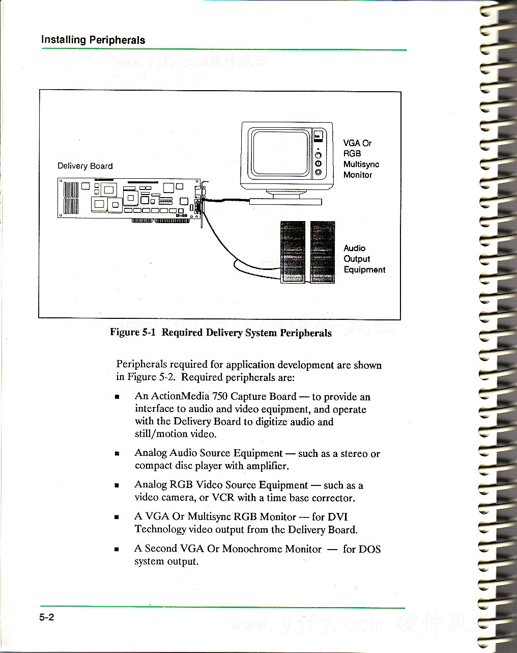
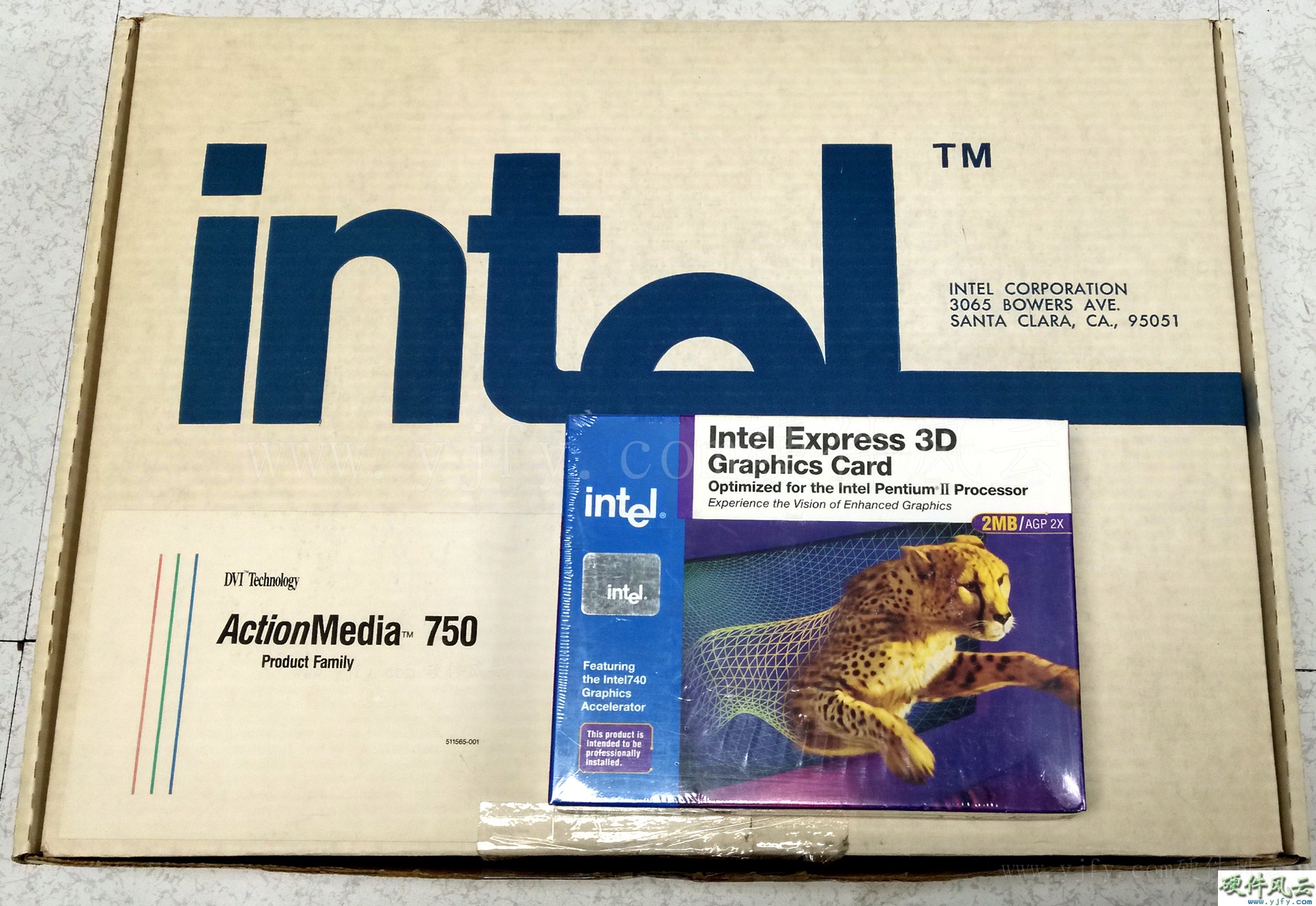
2.1 ACTIONMEDIA 750 Series Graphics Card
ACTIONMEDIA can be understood as universal media. The first
generation of ACTIONMEDIA graphics cards was the migration of Intel Pro
750 commercial digital media development technology to the consumer
consumption digital multimedia graphics card ACTIONMEDIA 750.
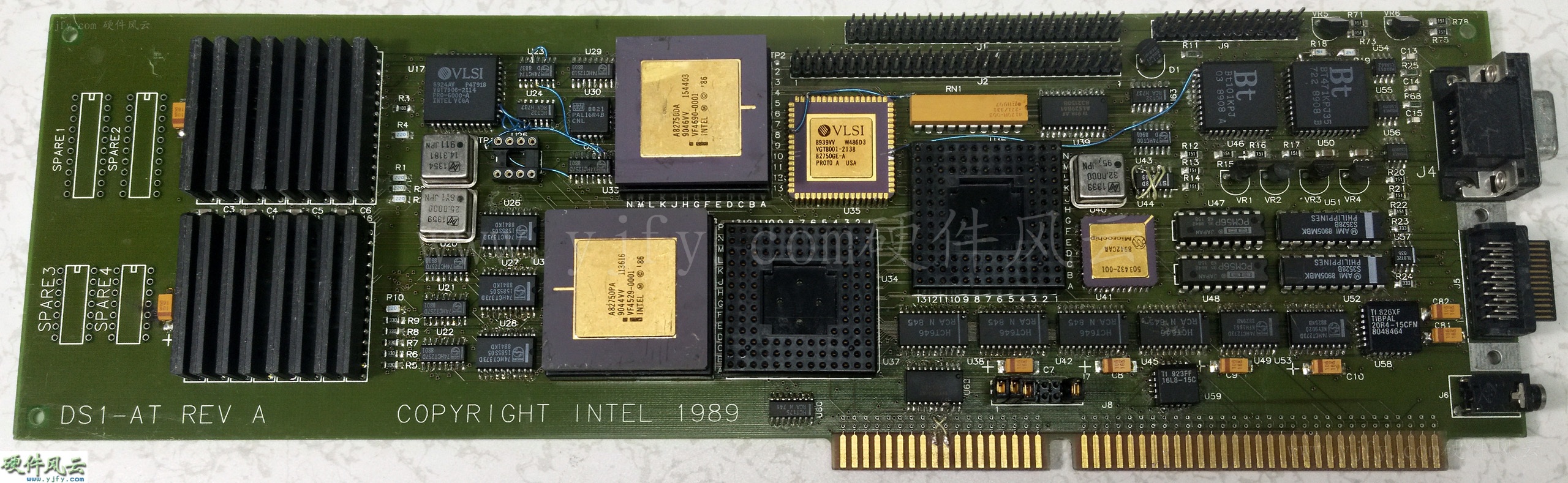
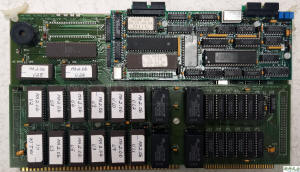
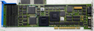
2.1.1 ACTIONMEDIA 750 Prototype Card DS1AT
In March 1987, a chip evaluation board for the i750 chip, codenamed
Tower, was made.The i750 product evaluation board DS1 was not developed
until 1989.The CS1 Delivery Board is matched with the DS1Capture Board.
DS1-AT is the ISA interface version prototype card. This board is
missing the original i750 chip, specially purchased the Intel i750PA/DA
chip, and the other two are missing VLSI VTG8001/8002.
DS1-AT Prototype
DS1-AT & CS1AT
The board below is a blank PROTOTYPE board without a chip.Also very
rare.
DS1-AT PCB Board
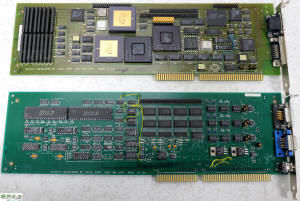
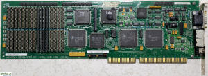
2.1.2 ACTIONMEDIA 750 ISA Version Engineering Sample
The ACTIONMEDIA 750 attracted widespread attention after its display
at the COMDEX/Fall '89 show from November 13 to 17, 1989.
ACTIONMEDIA 750 Engineering Sample

ACTIONMEDIA 750 & CS1AT
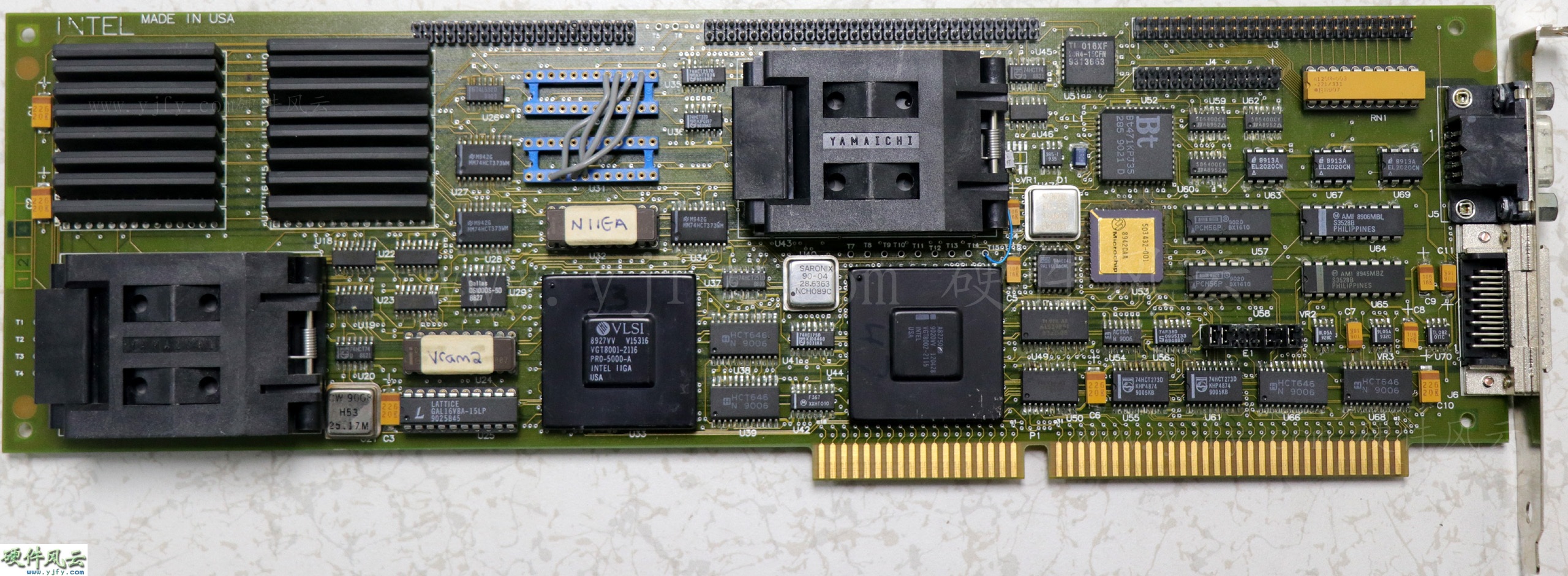
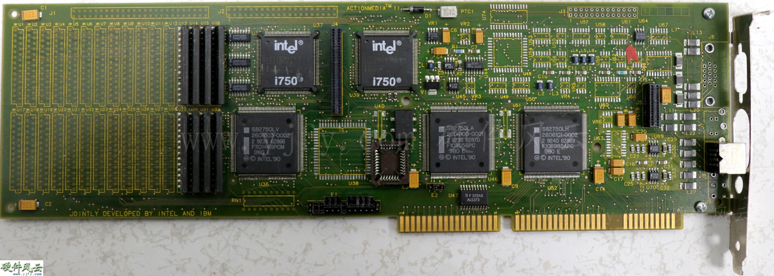
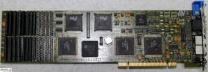
2.1.3 ACTIONMEDIA 750 MCA Version Engineering Sample
The MCA interface ACTIONMEDIA 750 DVI once appeared on behalf of
the ACTIONMEDIA series on March 5, 1990, "INFO WORLD", the only
ACTIONMEDIA 750 DVI picture that can be seen on the Internet.
ACTIONMEDIA 750 MCA Version Engineering Sample
ACTIONMEDIA 750 MCA & CS1MCA
2.1.4 ACTIONMEDIA 750
At that time, both Intel Pro 750 and ACTIONMEDIA 750 were "Only
available in limited quantities", making it difficult to see pictures of
these products.
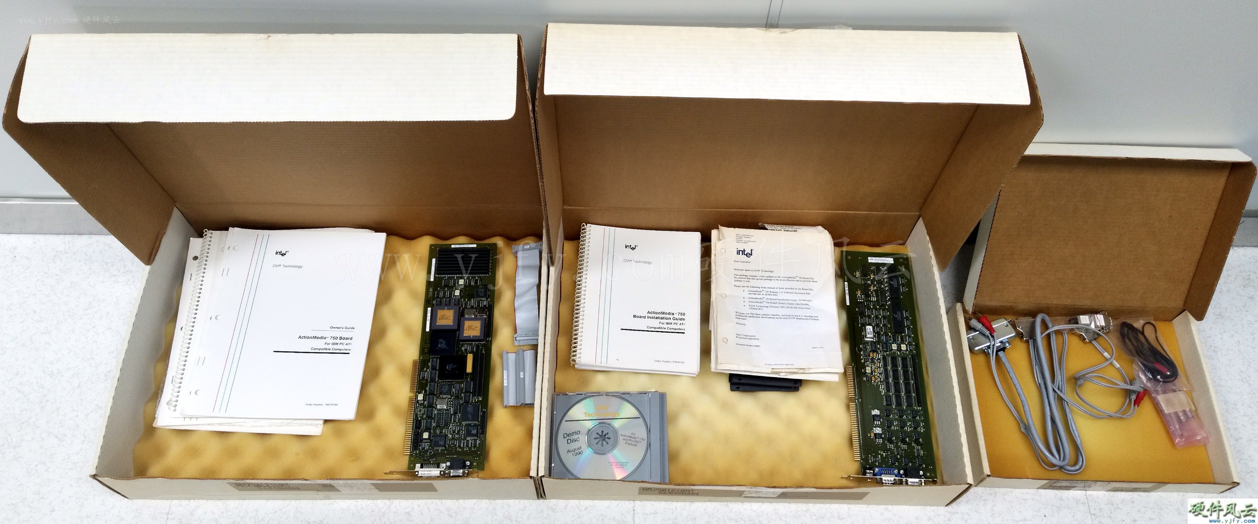
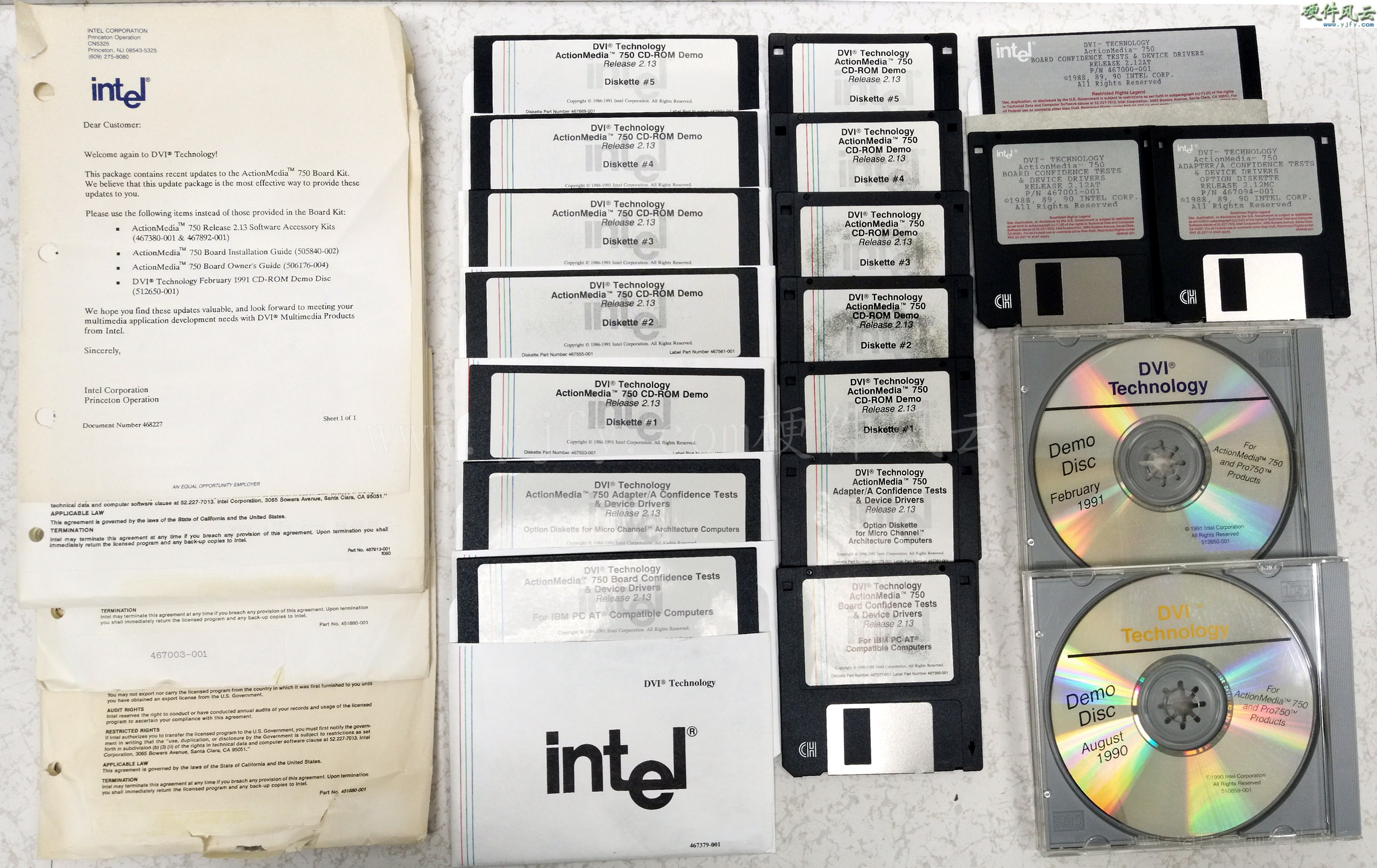
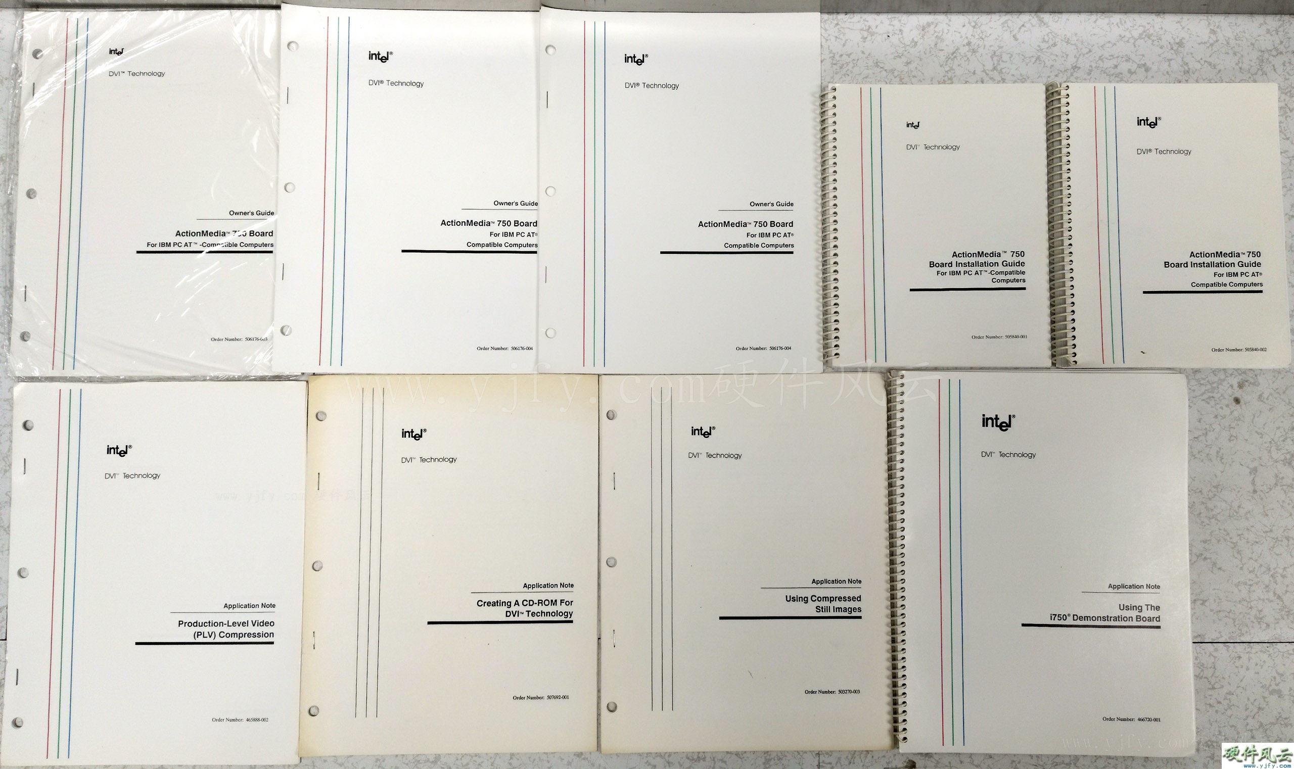
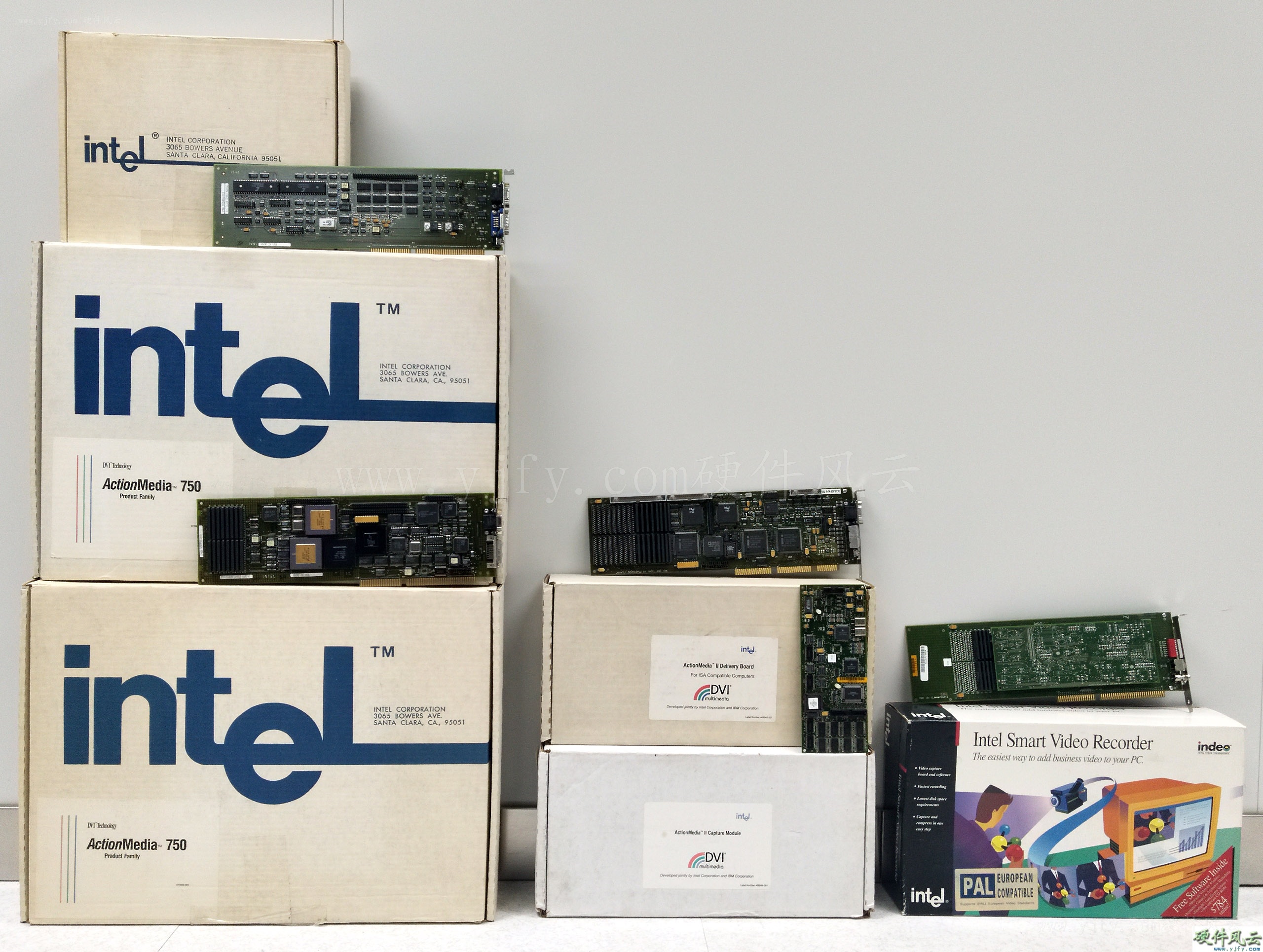
The picture below shows the boxed ACTIONMEDIA 750, with a lot of
floppy disks, CDs and manuals attached.
ACTIONMEDIA 750 Qualified Product
The ACTIONMEDIA 750 documentation contains the prototype card
information for ACTIONMEDIA II. It can be seen that the ACTIONMEDIA 750
is just a transitional product. This buyer spent $9,998 to buy but has
never used it.
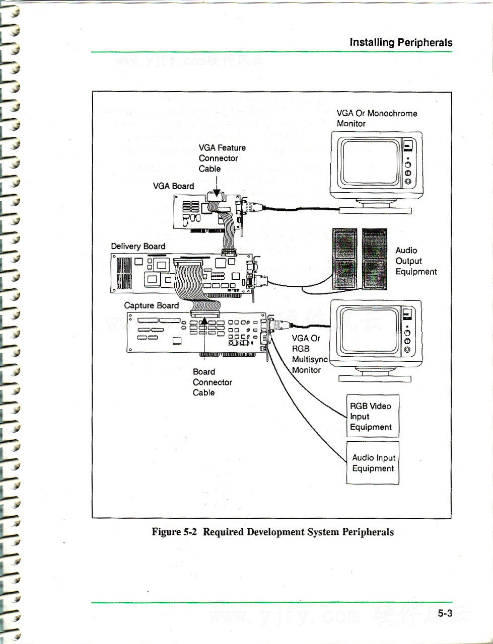
The following is a schematic diagram of the connection used. It can be
seen that the ACTIONMEDIA 750 can be used as a discrete graphics card.

The ACTIONMEDIA 750 documentation contains the prototype card information
for ACTIONMEDIA II. It can be seen that the ACTIONMEDIA 750 is just a
transitional product. This buyer spent $9,998 to buy but has never used
it.
The following is a schematic diagram of the connection used. It can be
seen that the ACTIONMEDIA 750 can be used as a discrete graphics card.
The boxed ACTIONMEDIA 750 has 3 boxes, which are quite large. Below is
a comparison of the boxed cards of the ACTIONMEDIA series. The first
column is ACTIONMEDIA 750, and the second and third columns are the
ACTIONMEDIA II and Smart video Recorder in the next section.
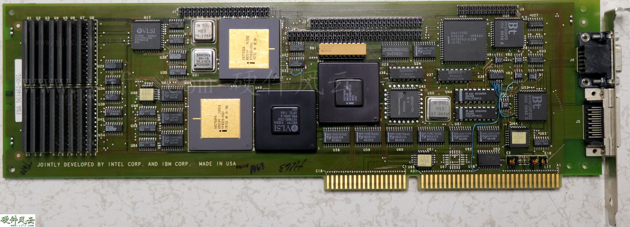
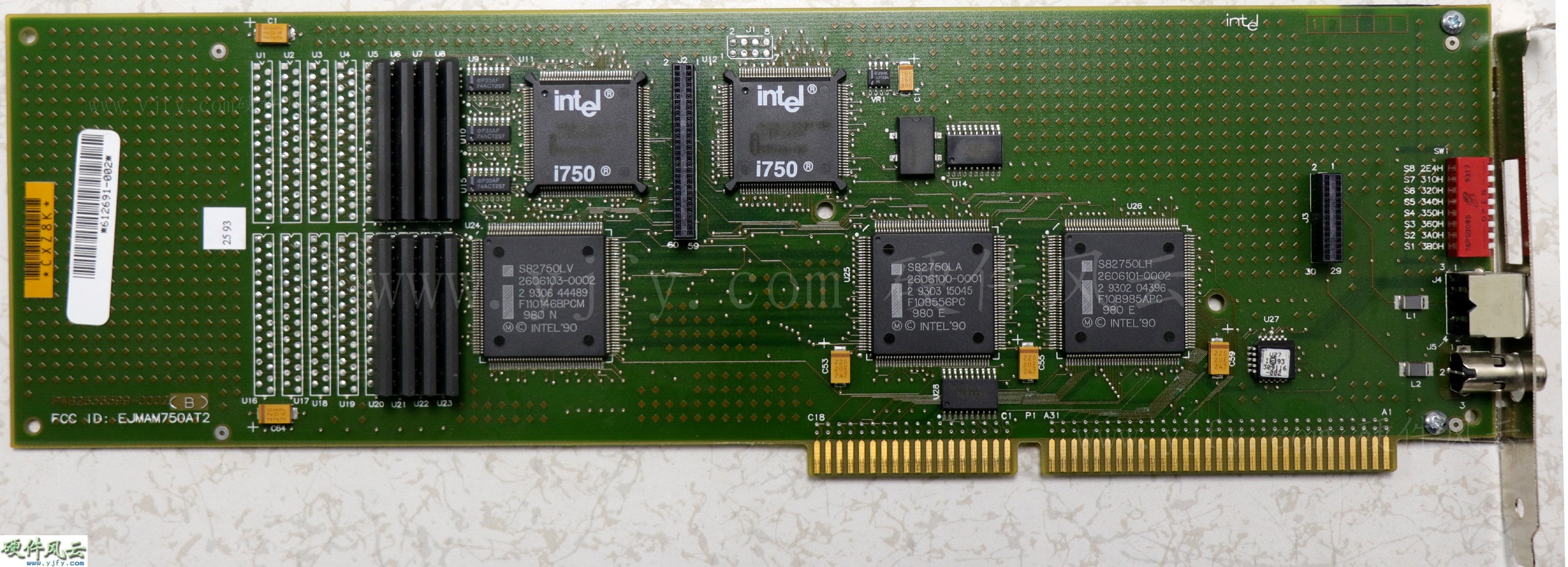
2.2 ACTIONMEDIA II Series Graphics Card
In the late 1980s, the patch manufacturing process of the board was
mature, and intel was naturally the leader. The i750PA/DA chip of the
PGA pin structure is upgraded to the i750PB/DB chip of the PQFP chip
structure, and the chip package is changed from a gold seal to a plastic
package.
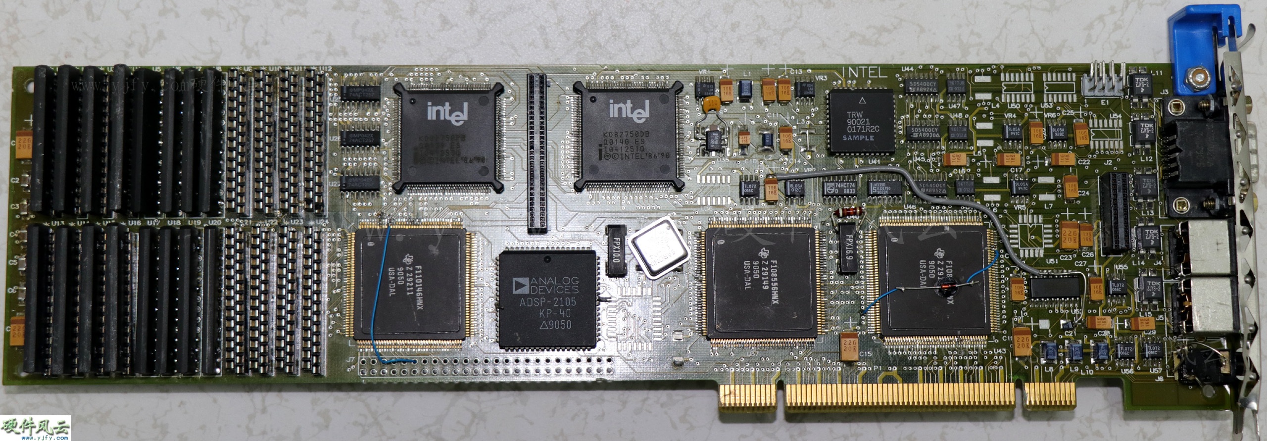
2.2.1 INTEGRATOR Chip Evaluation board
Based on the mature design of the previous generation, the chip
evaluation board INTEGRATOR was developed. So the INTEGRATOR looks like
the ACTIONMEDIA 750 DVI for the replace chip, or the CS1 card.
INTEGRATOR Chip Evaluation board

The ISA interface version of the detachable Chip Evaluation board INTEGRATOR's two i750PB/DB chips are ES.
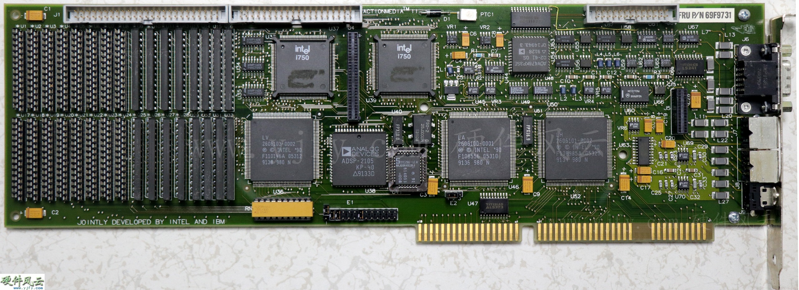
2.2.2 INTEGRATOR Chip Evaluation Board MCA Version
The figure below shows the INTEGRATOR of the MCA interface version.
The i750PB/DB ES chip date is very early.
INTEGRATOR Chip Evaluation board MCA Version
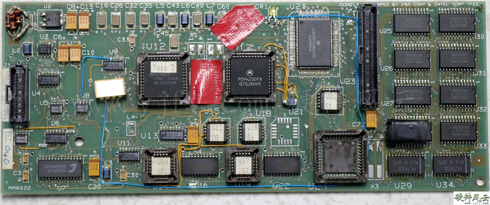
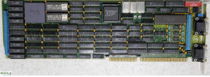
2.2.3 DS2AT Product Evaluation board
ACTIONMEDIA II was released on October 17, 1991 and was exhibited at
COMDEX Fall '91 on October 21-25, 1991 and won the Best of Show Award
and Best Multimedia Product Award. Intel's ACTIONMEDIA II graphics card
is to further optimize the structure of the ACTIONMEDIA 750 DVI primary
and secondary cards as the main daughter card structure, and also
designed three QFP-structured i750 series auxiliary chips for the
i750PB/DB chip. These 5 chips are:
82750PB pixel processor
82750DB display processor
82750LA Keying and Audio Gate Array (KAGA)
82750LH Host Interface Gate Array (HIGA)
82750LV VRAM SCSI Capture Gate Array (VSCGA)
DS2AT Product Evaluation board
CS2
Prototype

2.2.4
DS2MCA Product Evaluation board
The ACTIONMEDIA II Product Evaluation board is codenamed DS2. The
following MCA interface version ACTIONMEDIA II is DS2MCA, which has five
i750 chips. The i750PB/DB is obviously the ES version. The only three
codes of the ceramic seal are not the unlabeled models. It is the ES
chip of the early i750LA/LH/LV.
DS2MCA Product Evaluation board
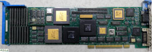
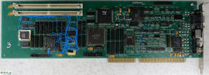
2.2.5 ACTIONMEDIA II Engineering Sample ISA Version
ACTIONMEDIA II Engineering Sample ISA Version
2.2.6 ACTIONMEDIA II Engineering Sample MCA Version
ACTIONMEDIA II Engineering Sample MCA Version
CS2 Engineering Sample
2.2.7 ACTIONMEDIA II Qualified Product
ACTIONMEDIA II Qualified Product
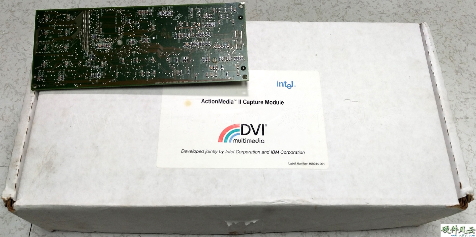
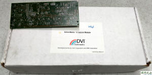
Capture module
|
|
2.3 ACTIONMEDIA III Series Graphics Card
Around 92 years, Intel began to develop ACTIONMEDIA III.ACTIONMEDIA
III was originally designed to be the same as the ACTIONMEDIA II as the
main daughter card structure, and later adjusted to a single card.
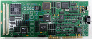
2.3.1 QUARK Chip Evaluation Board
ACTIONMEDIA III should update the i750PB/DB and launch the i750PC/DC
Chip Evaluation board. In fact, it is an evaluation of the update of the
auxiliary chip. Presumably, the chip to be evaluated integrates the
functions of the original 82750LA, 82750LH, and 82750LV3 chips. The chip
to be evaluated should be i750SN, which will be introduced later.
QUARK Chip Evaluation Board
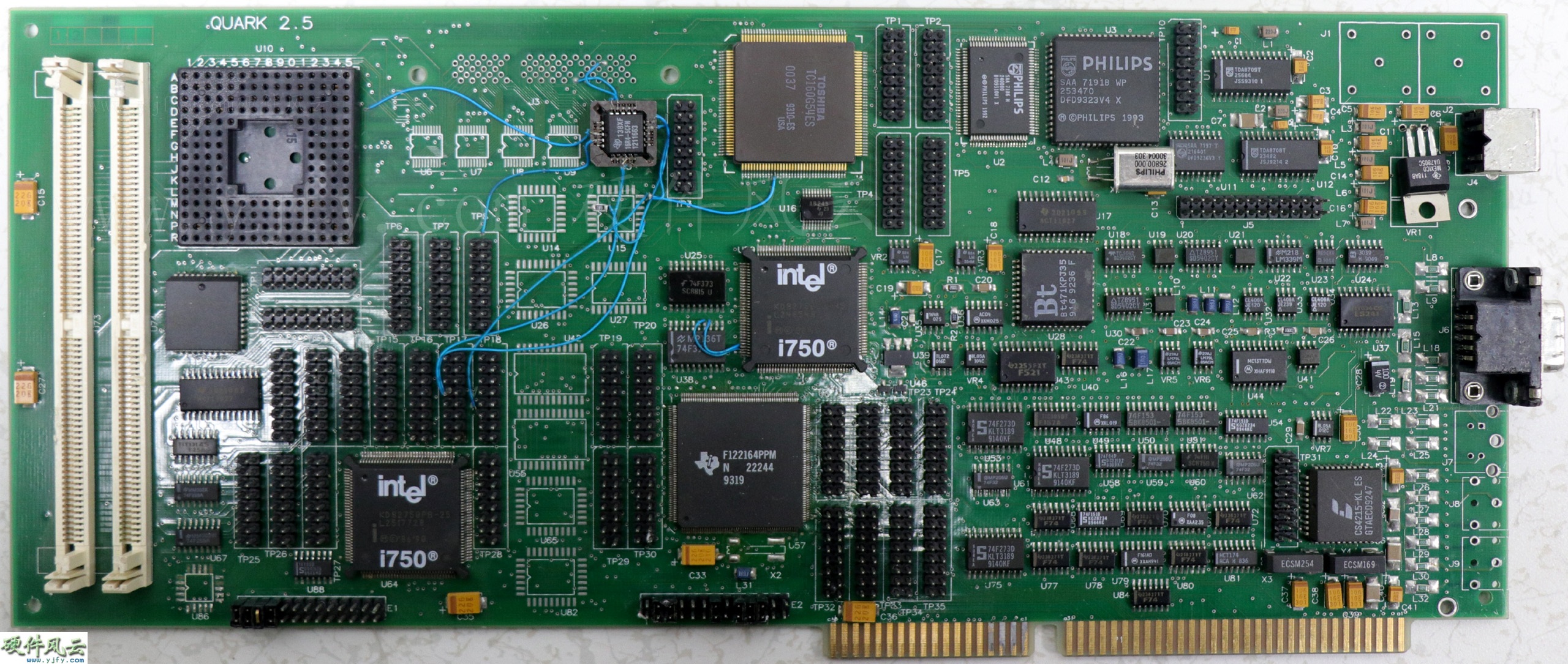
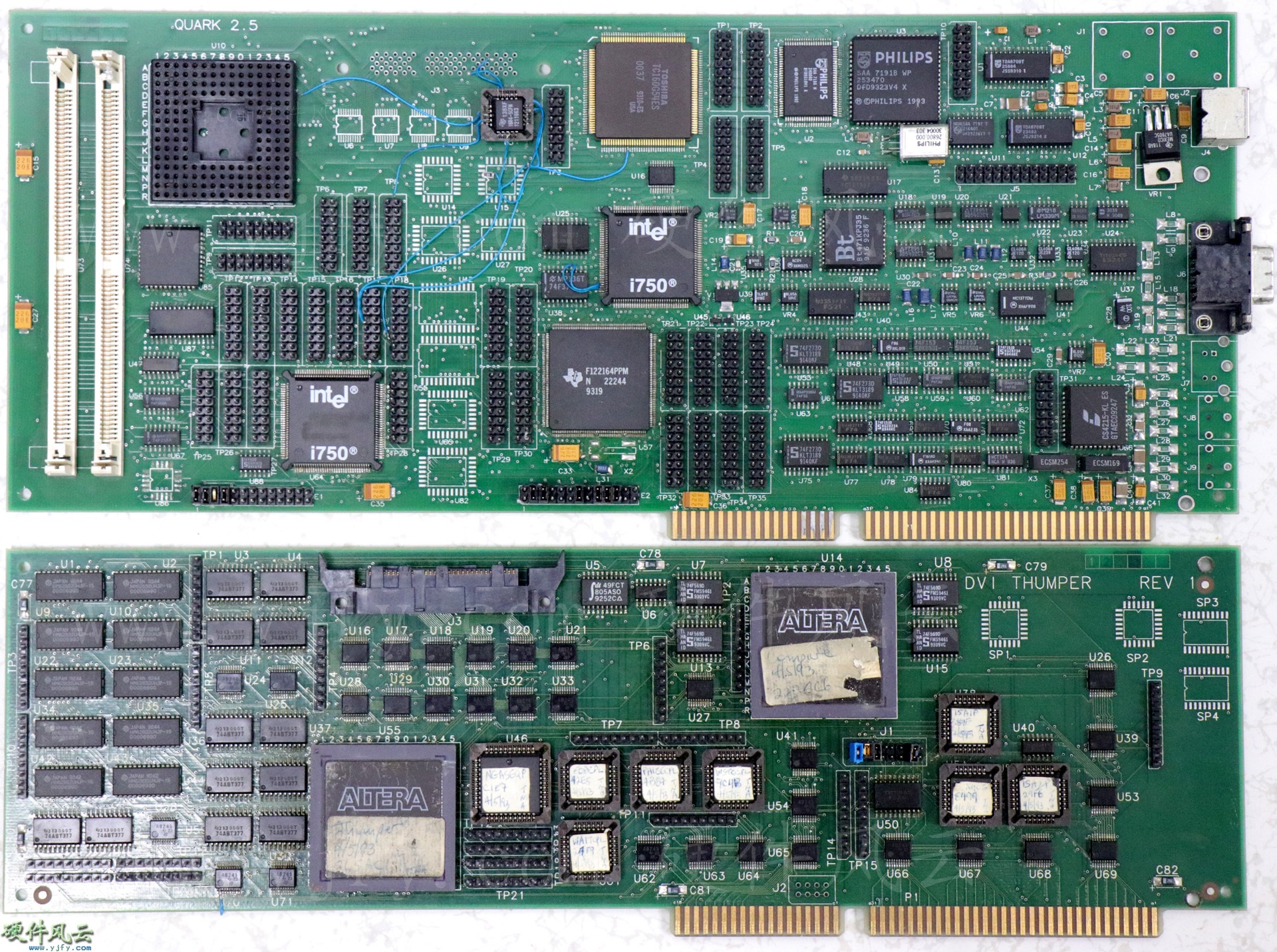
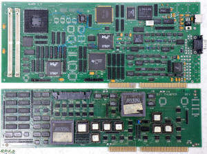
2.3.2 QUARK II Chip Evaluation Board
QUARK II Chip Evaluation Board
QUARK's REV 2 version compared with the above REV 1 version, QUARK's REV
2 version of the chip evaluation board is about one-third wider than the
REV 1 version of the standard ISA full-length board, the extra place is
loaded two One function, one on the right, is the function chip
evaluation board area of the daughter card, and the function of the
daughter card is directly extended on the main card. As the integration
level is improved and the memory is processed in two slots, the ISA
interface master card has enough functions to directly accommodate the
daughter card, and the daughter card function can be cut by the empty
soldering。
Chip evaluation board QUARK 2.5 chip in order i750PB, i750DB,
F122164PPM and TC160G54ES, this TC160G54ES chip is very special, Intel
not only set a PGA chip socket on the graphics card, but also equipped
with a DVI THUMPER secondary card to deploy. This interface has not been
made on the QUARK 2.5 graphics card, but the above socket can be
indirectly debugged using Altera's EPM7192GC160-1 PGA chip that has been
processed by the DVI THUMPER secondary card.
QUARK II Chip Evaluation Board & DVI THUMPER
The i750 chip project began in 1986 with the i750PA/DA chip, and finally
the 1993 i750PD chip, which lasted 8 years. The i750 chip was
undoubtedly excellent at the beginning of its birth. Intel did not
update or replace the PCI interface. In the latter stage, its excellent
performance index became a congenital deficiency. In the end, it had no
potential to be dug and had to end. The 2D graphics project of Intel's
i750 chip is also finished. This was followed by the development of
video cards.
2.4 i750PD Chip
ACTIONMEDIA III did not routinely develop the i750's
third-generation i750PC/DC chip, resulting in the
vacancy of the i750PC/DC numbering chip. The fourth
generation is the i750PD (Video Compression Processor)
chip.
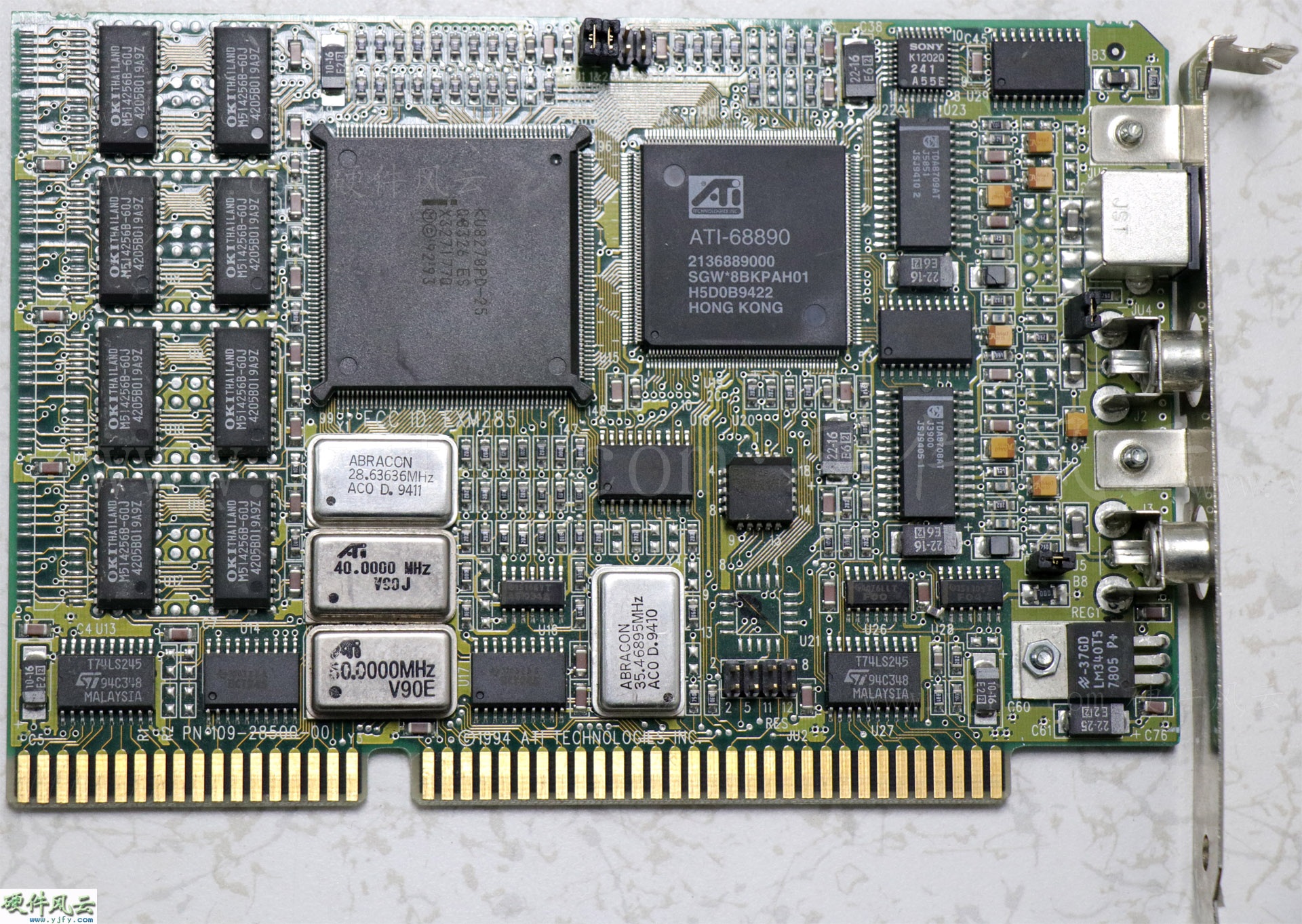
On November 15, 1993, ATI announced the Video basic
capture card, which uses Intel's low-cost i750PD and
ATI's ATI-68890 video capture chip. The chip below shows
the ATI Video basic capture card is ES, the chip is
labeled KU8270PD-25, it seems to be marked incorrectly,
it should be KU82750PD-25.
ATI Video basic capture card Qualified Product

2.5 MAESTRO series
The late stage of the i750 chip graphics project,lintel did not
completely abandon the research and development of the i750 chip
follow-up products, turned to simplified functions, low-cost video
daughter cards and committed to selling i750 series chips to large
companies such as ATI and Creative.
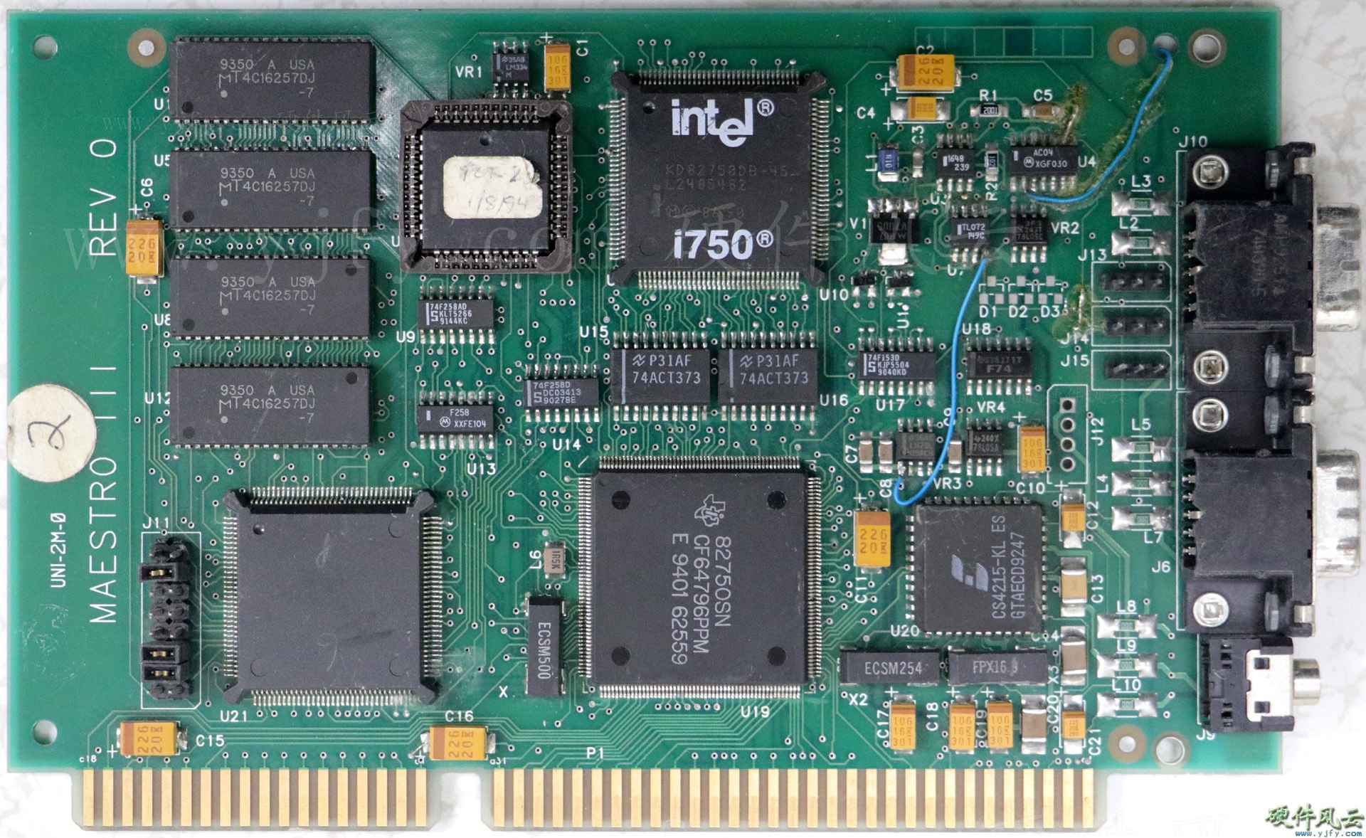
MAESTRO III Evaluation board
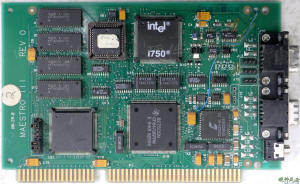
The MAESTRO III card has i750DB, i750SN and a chip without any label.
This chip without any standard should be the next generation chip,
because at this time Intel can not make the i750PB into a wordless
version of ES. The i750SN chip should be the F122164PPM on the QUARK
chip board.As can be seen from the date of the components used on the
card, the i750PE chip was made in early 1994. For some reason, the final
product of such a card structure has not been seen, or only the i750PE
chip is evaluated, and the chip is prepared for the Smart video Recorder
series.
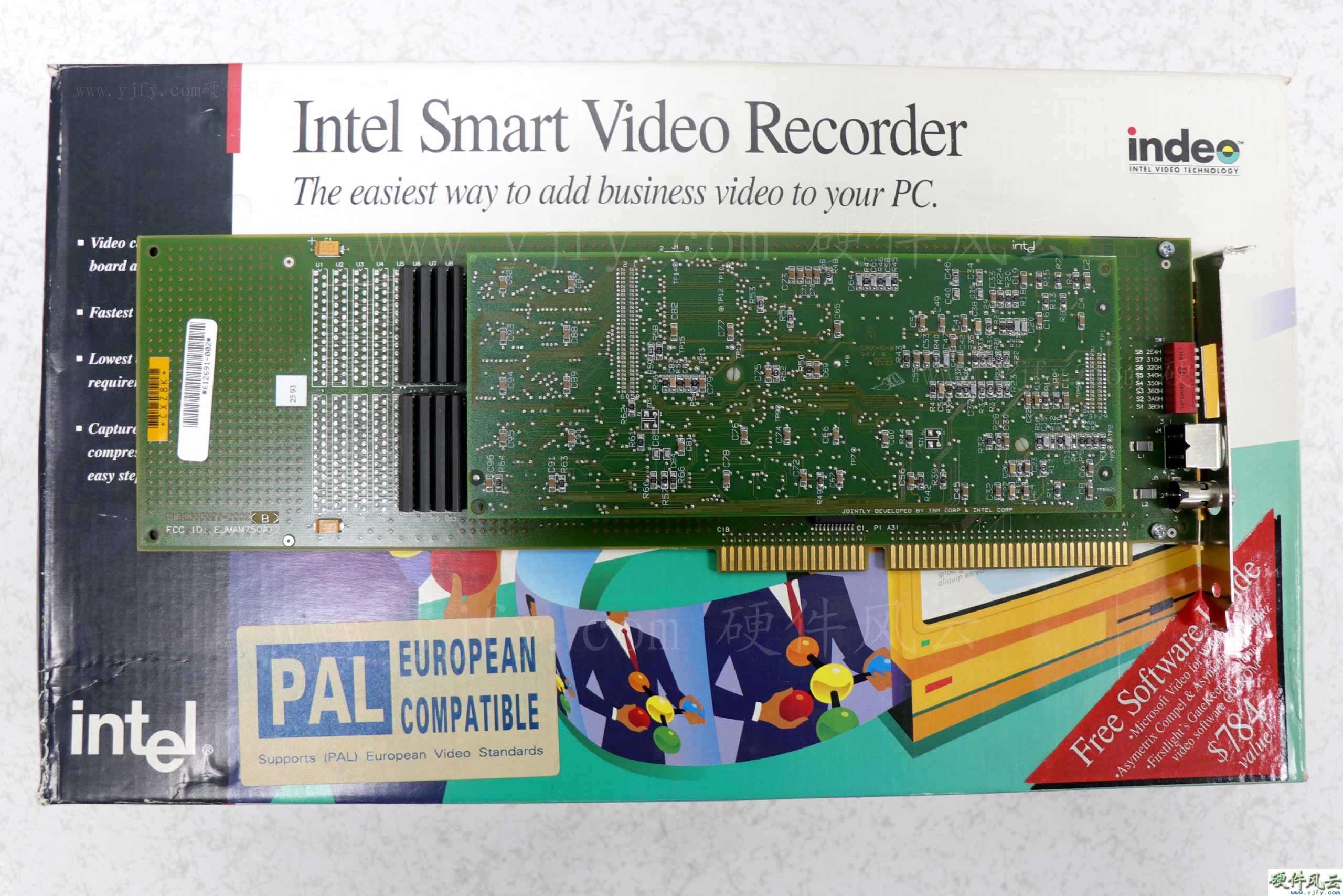
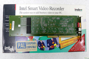
2.6 Smart video Recorder series
In the late stage of the ACTIONMEDIA II graphics card, INTEL removed
the graphics display function of ACTIONMEDIA II and turned it into a
Smart video Recorder series video capture card. Smart Video Recorder
literally means a smart recorder that captures and compresses video
analog signals into digital video files for playback and editing.
2.6.1 Smart video Recorder Product Evaluation board
Smart video Recorder Product Evaluation board

2.6.2 Smart video Recorder Qualified Product
Smart video Recorder Qualified Product
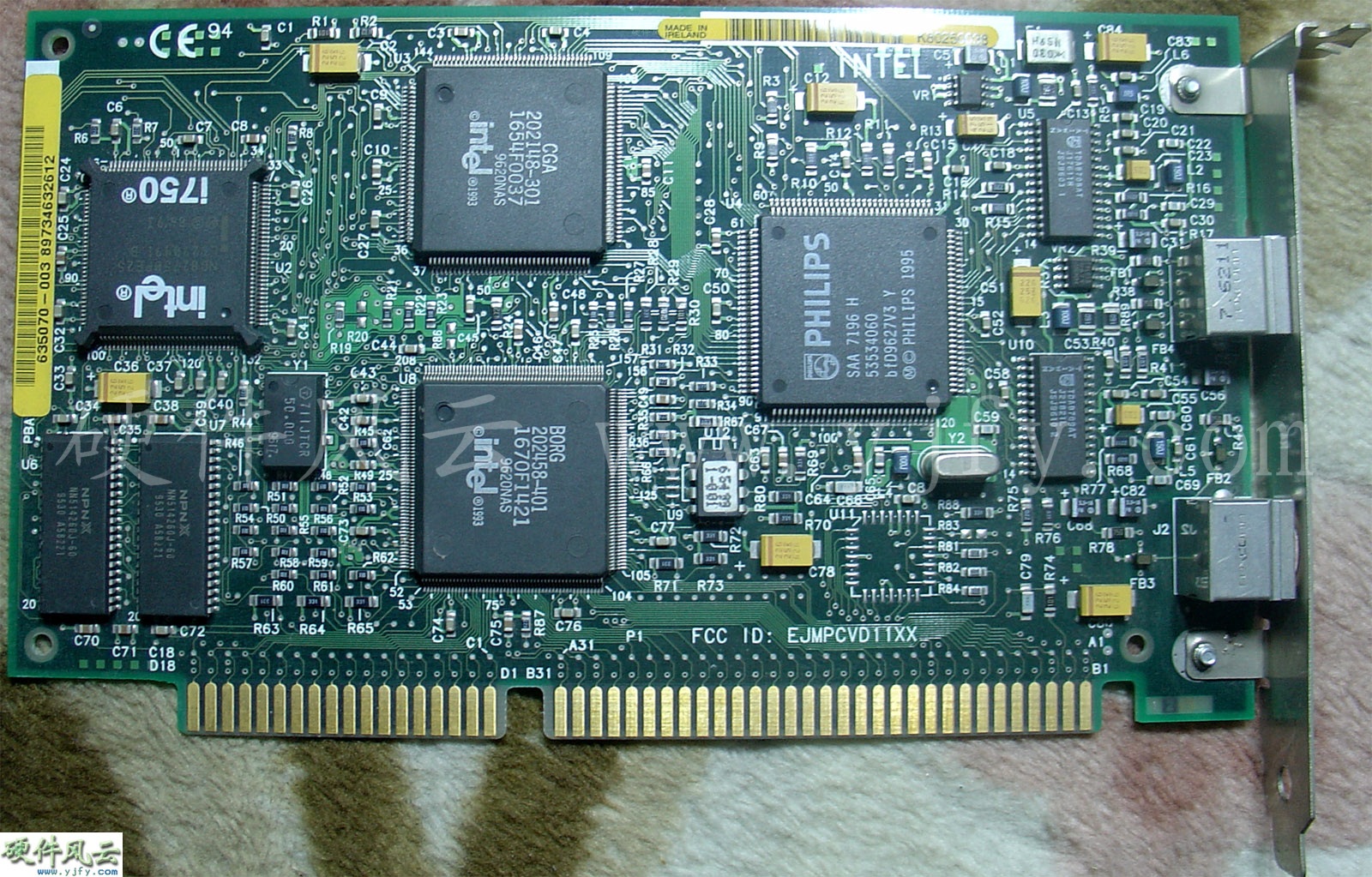
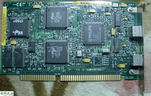
2.6.3 Smart video Recorder pro
Although the ACTIONMEDIA III and MAESTRO projects were aborted, the
BORG, CGA and i750PE chips were provided for the Smart video Recorder
pro.Creative has similar products available.
SMART VIDEO RECORDER PRO Qualified Product
2.6.4
Smart video Recorder III
Smart Video Recorder III does not use INTEL's i750 series chips, nor
is it the ISA/MCA interface used by INTEL's first-generation graphics
cards. A PCI-based Smart Video Recorder III video card made an
inexplicable end to INTEL's first-generation graphics card in 1996.
Smart video Recorder III Qualified Product
Intel's first-generation graphics project began in 1989 with ACTIONMEDIA,
and finally in 1996 the Smart Video Recorder III, which lasted eight
years. Because the products are rarely seen on personal computers, their
popularity is so low that they are forgotten. |
|
3. 2 years of granding (1997-1998)
Intel's
first generation of discrete graphics cards is based on the i750 chip
ISA / MCA interface ACTIONMEDIA series graphics cards, and the second
generation of discrete graphics cards is based on i740 chip AGP
interface Express 3D series graphics cards. Intel did not develop a
display chip for the PCI interface it invented. Maybe it is Intel's
extreme confidence in the i750-based graphics card, or it may be that
its technology reserves are insufficient and it missed the era of PCI
graphics cards.
3.1 PCI graphic card
Although Intel did not launch a display chip based
on the PCI interface, there are still some PCI graphics cards related to
Intel.
3.1.1
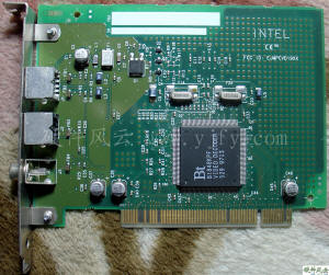
Purchase graphics chip
Querying
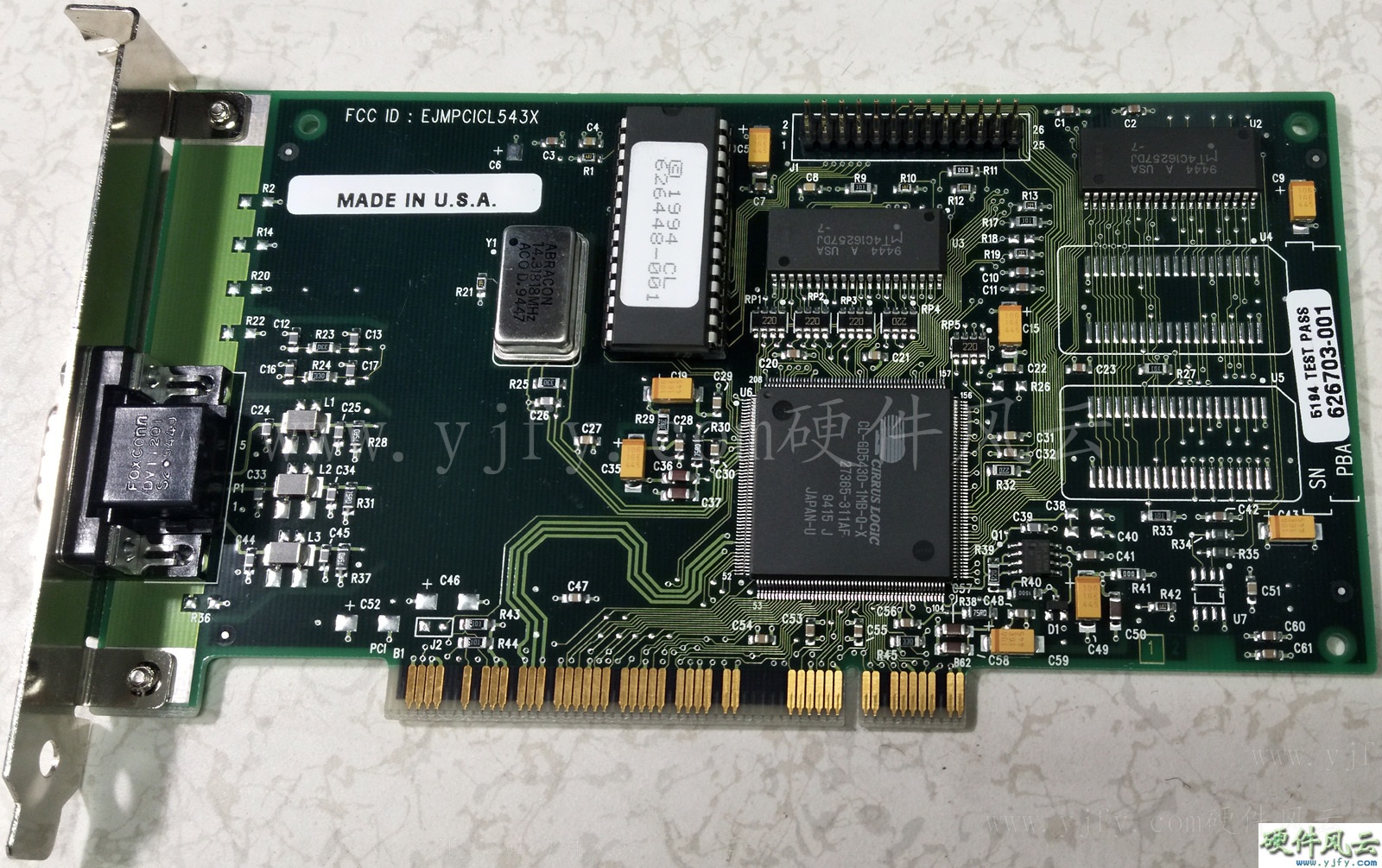
the FCCID shows that Intel has produced only one type of PCI graphics
card. Its FCCID: EJMPCICL543X is a CL-543X series chip using Cirrus
Logic. I have two models, one is a CL-5430 chip and the other is a
CL-5434 chip. This PCI graphics card Intel has been used in HP computers
in addition to its own use.
Intel PCICL5430
3.1.2 Purchase graphics card
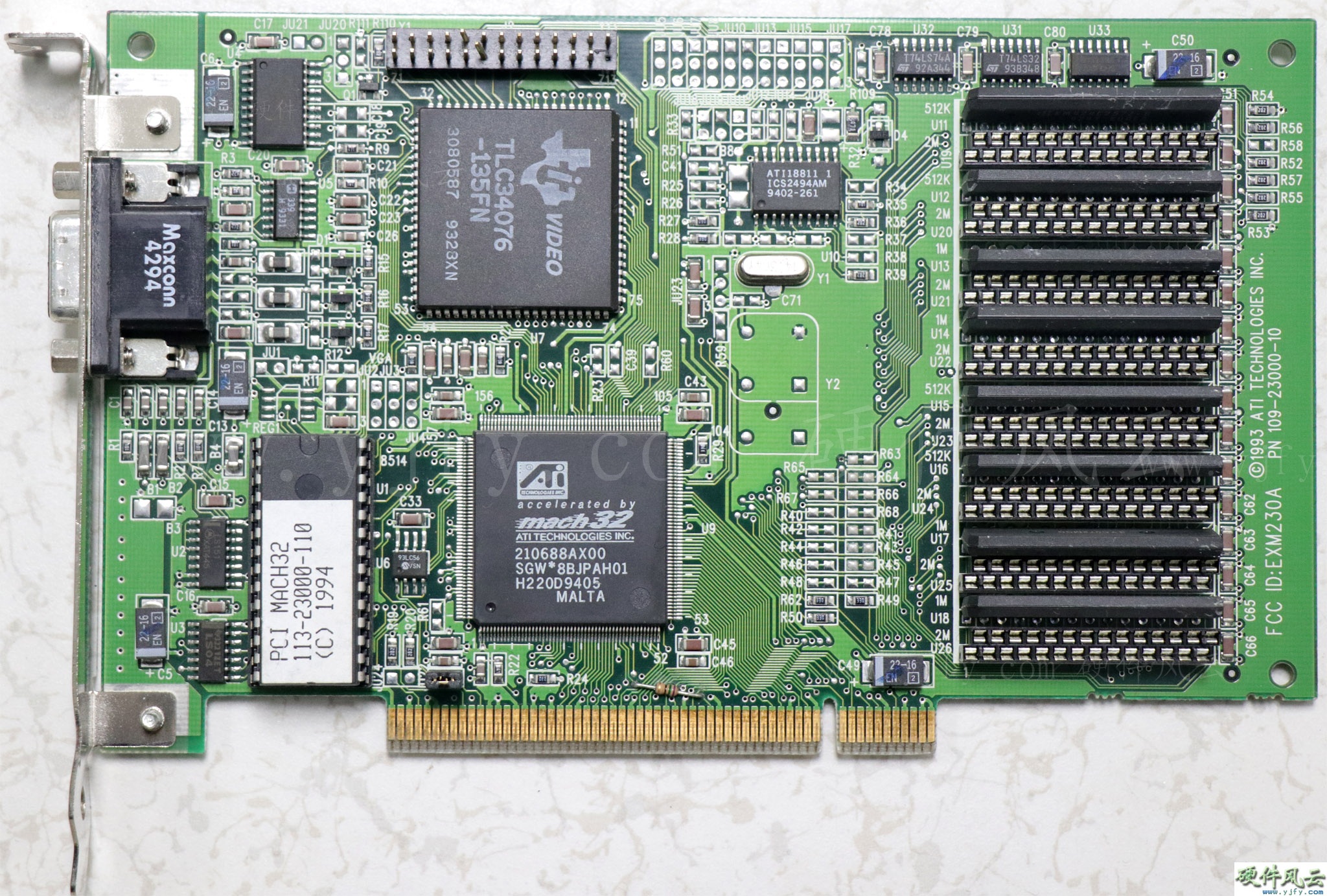
In the era of ISA graphics, Intel has used VIDEO 7 INC graphics cards.
Intel, Intel also directly purchased graphics cards from PCI cards, such
as ATi graphics cards.
ATi Mach32

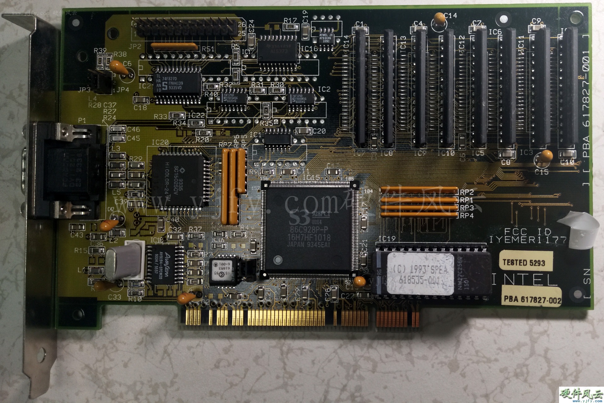
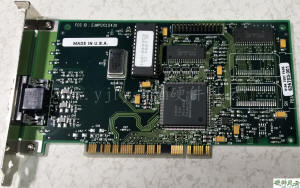
3.1.3 ODM graphics card
In the era of PCI graphics, Intel has a partnership with VIDEO 7 INC.
SPEA Software AG acquired VIDEO 7 INC. SPEA Software AG gives Intel ODM
PCI graphics cards.
Intel 928PCI

3.1.4 Acquisition of graphics card company
In order to acquire the relevant technology, in July 1997, Intel
acquired Chips & Technologies, which was the leader in 2D display design
and R&D. Intel's move is not only to avoid the embarrassing situation
that no graphics chip is available in the era of PCI graphics, but also
a sign of vigorously entering the graphics card market.
Chips
& Technologies/Intel
DKHIQV-PCI
BOARD
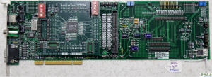
This DKHIQV-PCI Development board has an "INTEL" label.
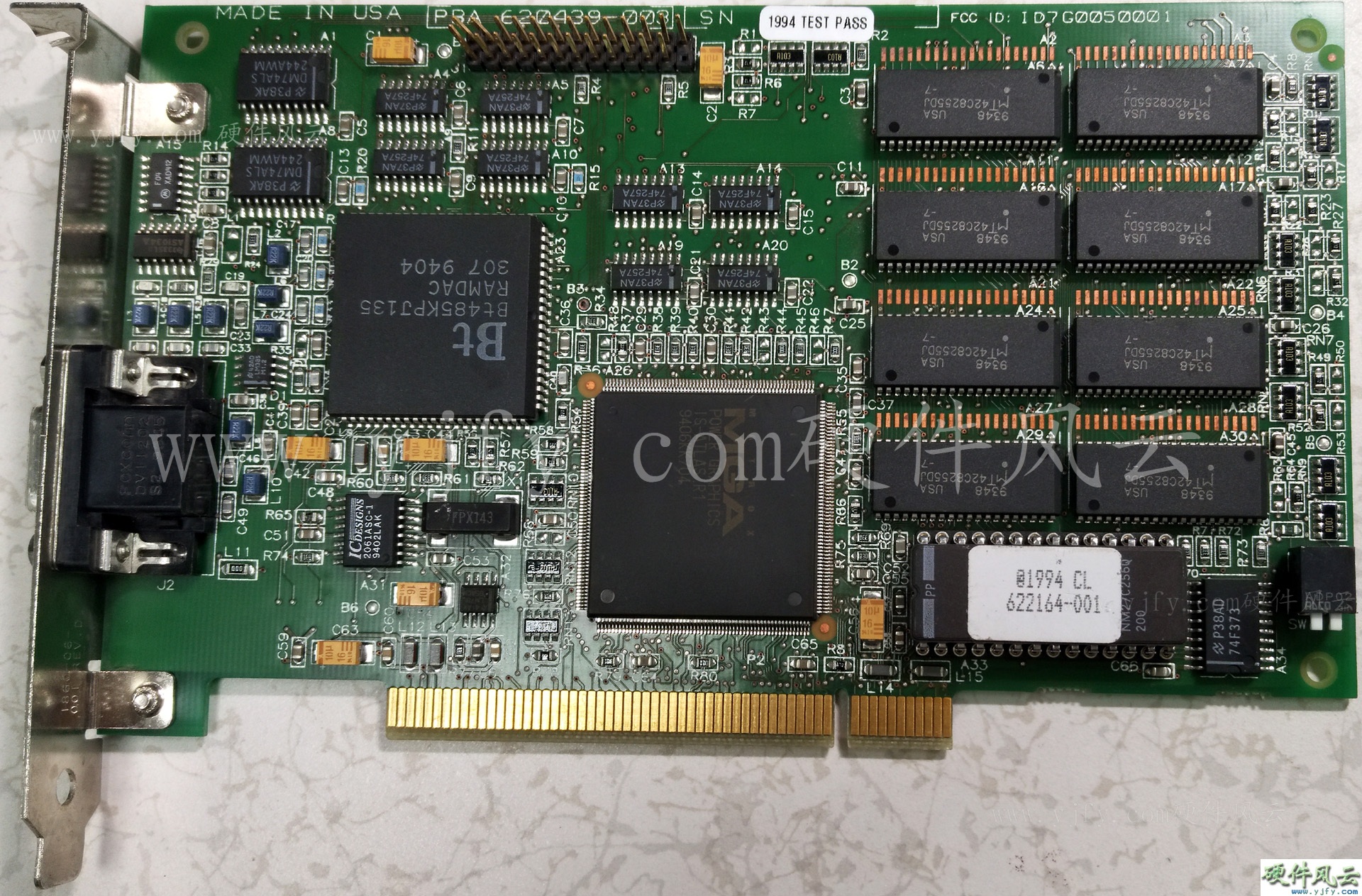
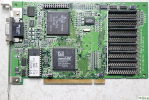
3.1.5 Clone graphics card
Intel has cloned MATROX's Ultima graphics card. This card has lntel's
PBA 620439-003 and Matrox's FCCID: ID7G0050001, which is only used
inside Intel.
lntel/MATROX Ultima
3.2 i740 chip series graphics card
Intel's second-generation discrete graphics card began in the second
half of 1997 with the AGP interface graphics card developed by Intel and
Real3D, codenamed "Auburn", and was released in January 1998.
The i740 chip is manufactured in a 0.35 micron process and is a 64Bit
graphics core with a core operating speed synchronized to the AGP bus at
66MHz. The i740 chip is the first true AGP 2X graphics card. Supports up to
8MB of SGRAM/SDRAM memory. The pixel fill rate is 55M Pixels/s, the
triangle generation speed is 0.5-1M Trianglws/s triangle generation
speed is 5-10 million per second, and the 203MHz RAMDAC is built in.
Although the i740's 2D speed is average, its 3D performance is not bad,
and it can fully support hardware DVD playback.
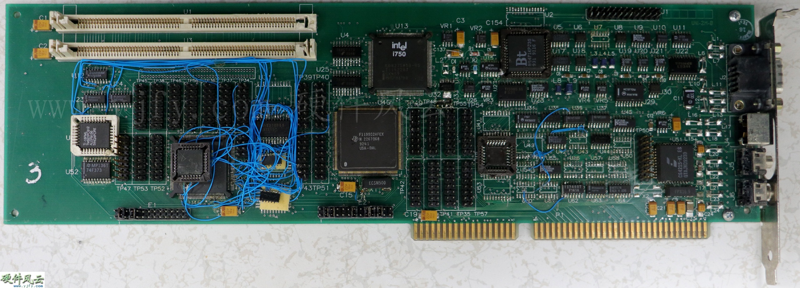
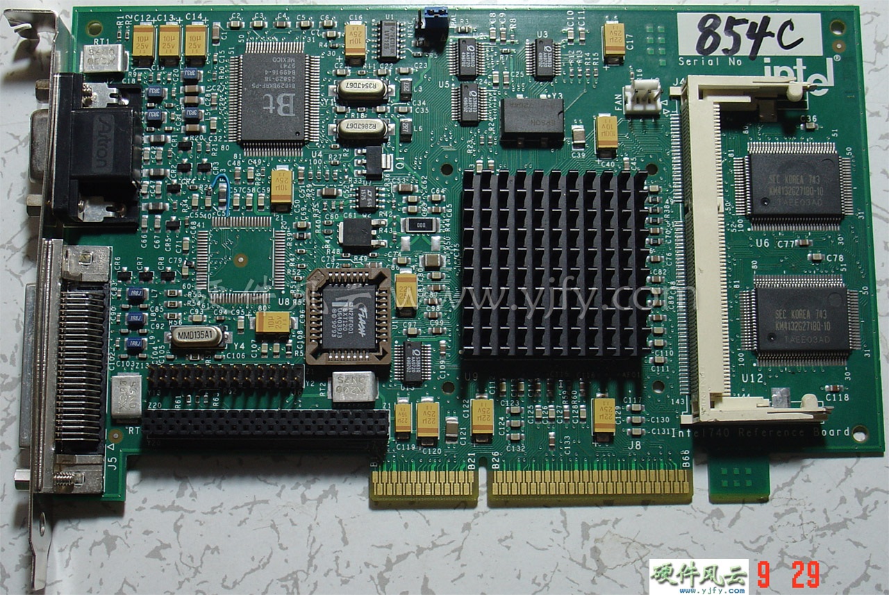
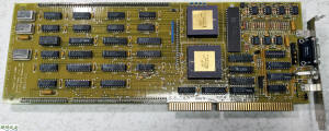
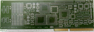
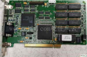
3.2.1 INTEL740 Evaluation board
The following picture shows the intel i740 chip evaluation board. The
right side of the front side of the PCB on the graphics card is marked
with the "INTEL740 Evaluation board". The PCB date was 3497 and it
appeared before August 1997.
INTEL740
Evaluation board
Although
the i740 chip was developed by Real3d, the chip is marked with Intel's
logo. It can be seen that intel pays attention to the i740 chip.
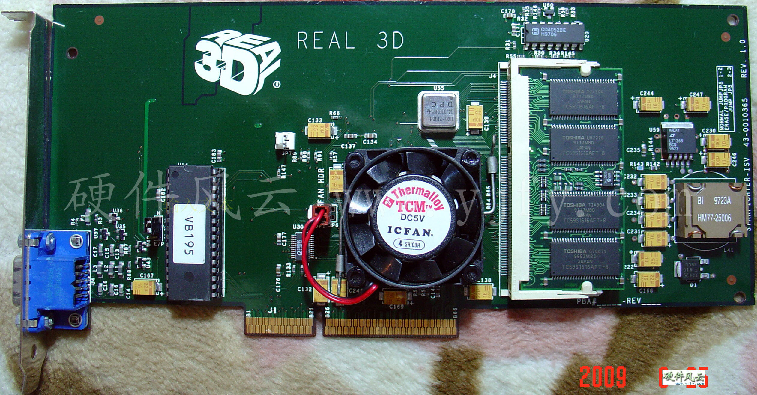
3.2.2 Real3D StarFighter-ISV Evaluation board
This is the chip evaluation board of the i740 chip SDRAM memory
version. It seems that Real3D and Intel are responsible for chip
evaluation of SDRAM and SGRAM versions respectively.
StarFighter-ISV Evaluation
board

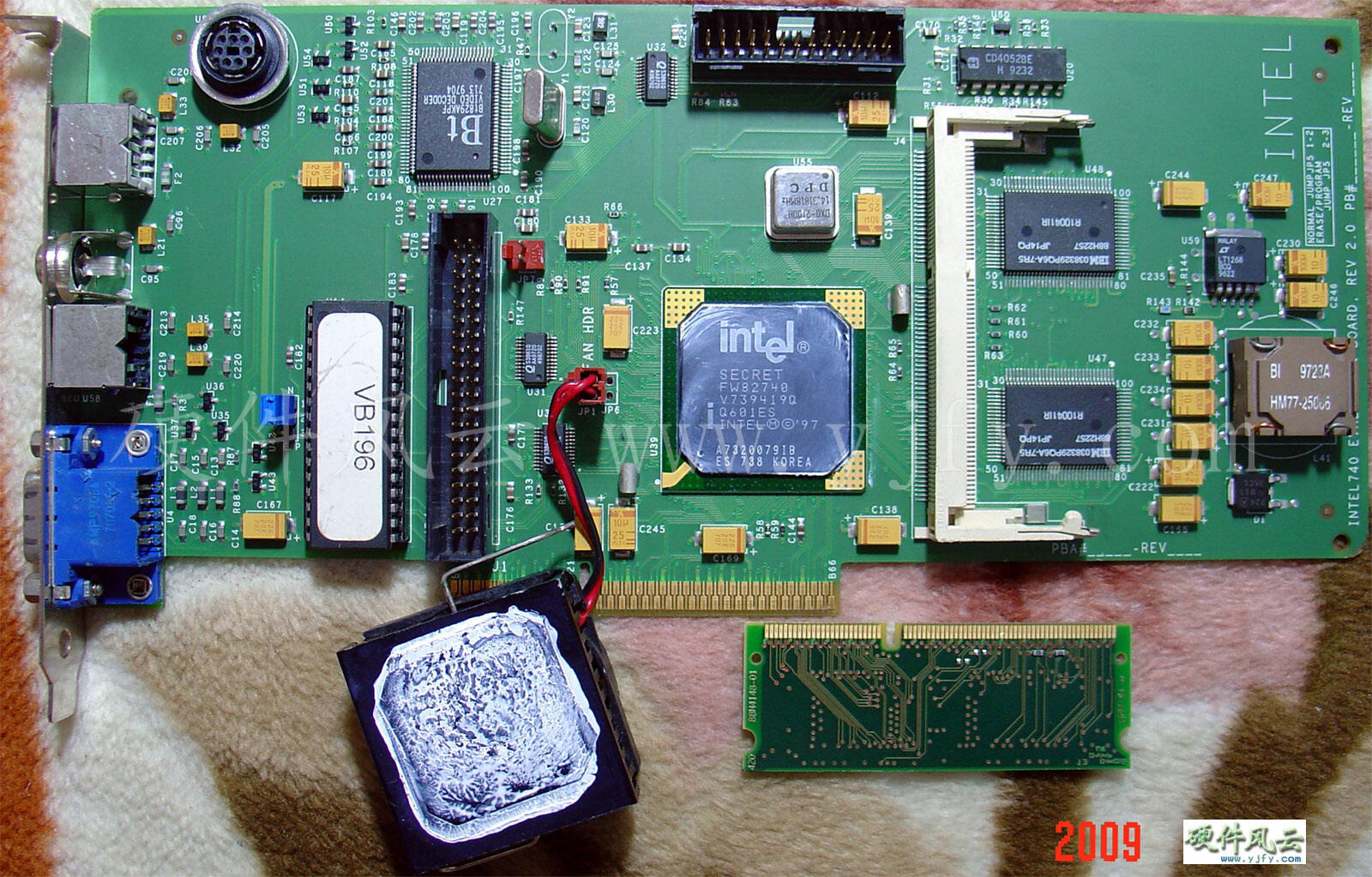
3.2.3
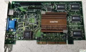
Intel740 Reference board
The front right side of the PCB on the Intel i740 graphics card is
labeled "INTEL740 reference board". Intel had planned to let other
manufacturers make graphics cards according to this reference design. In
fact, based on cost considerations, no one vendor used this luxurious
design, and even Intel itself launched Express 3D graphics cards to be
streamlined and streamlined.
INTEL740
reference board

3.2.4 Gainward Intel740 APAC Reference design
In order to promote the i740 chip graphics card, Intel regards
Gainward as the most important partner and commissions Gainward to
design the Intel740 APAC REFERENCE DESIGN in the Asia-Pacific region. So
it seems that Intel's own reference design is for the European and
American version. In fact, this Asia-Pacific version of Gainward has
never been used, nor is it used by other manufacturers. Why? Because in
this design, not only the PCB board size is the same as the European and
American version, it is very large, and the heat sink is also the
largest of the i740 chip graphics cards, none of them.
Gainward Intel740 APAC Reference design
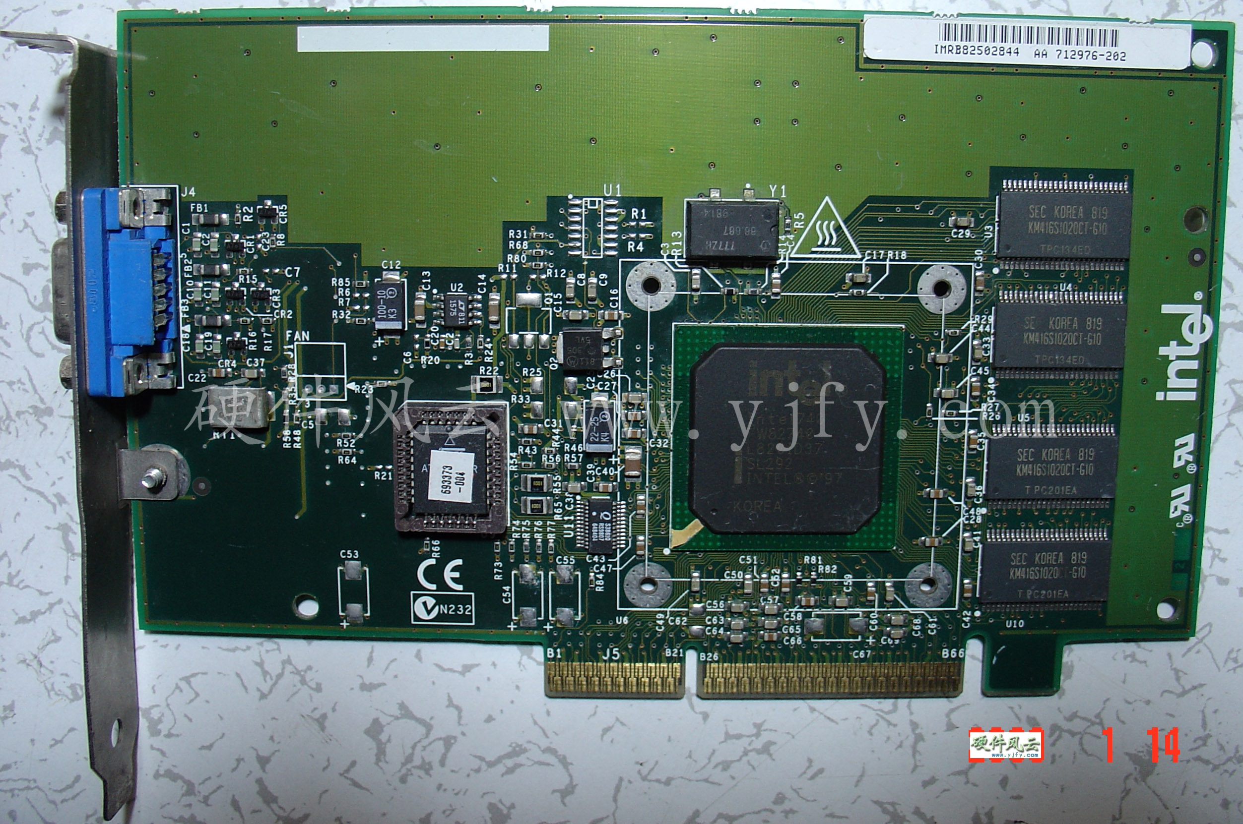
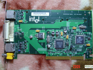
3.2.5 Express 3D
On April 15, 1998, Intel officially released the express 3D graphics
card, which is the first generation of Intel independent graphics card
commonly used on the Internet. After reading the previous information, I
think you will only agree that it is the first generation of Intel 3D
graphics card.
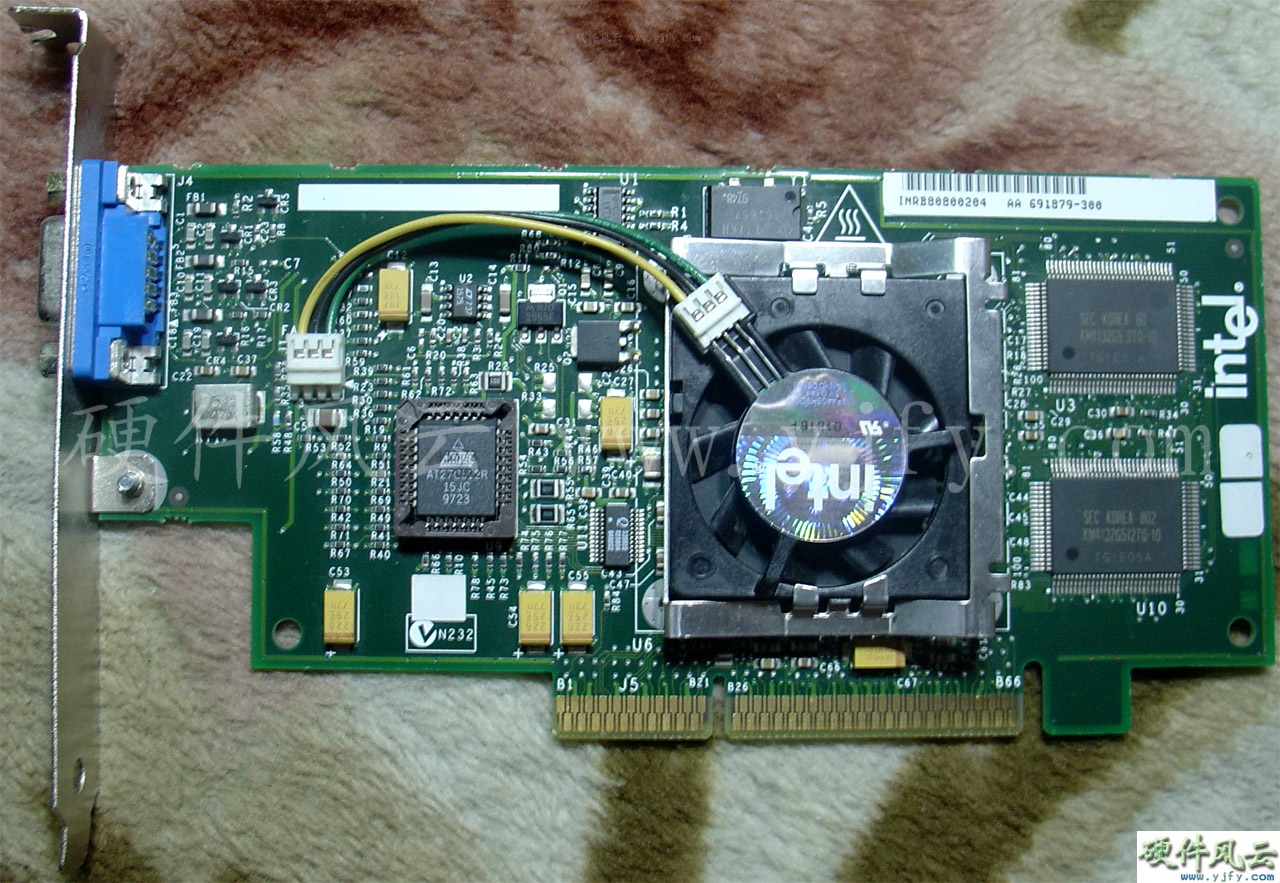
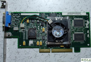
3.2.5.1 Express 3D Evaluation board
Product evaluation board for Express 3D, date of manufacture 9804.
Express
3D Evaluation board

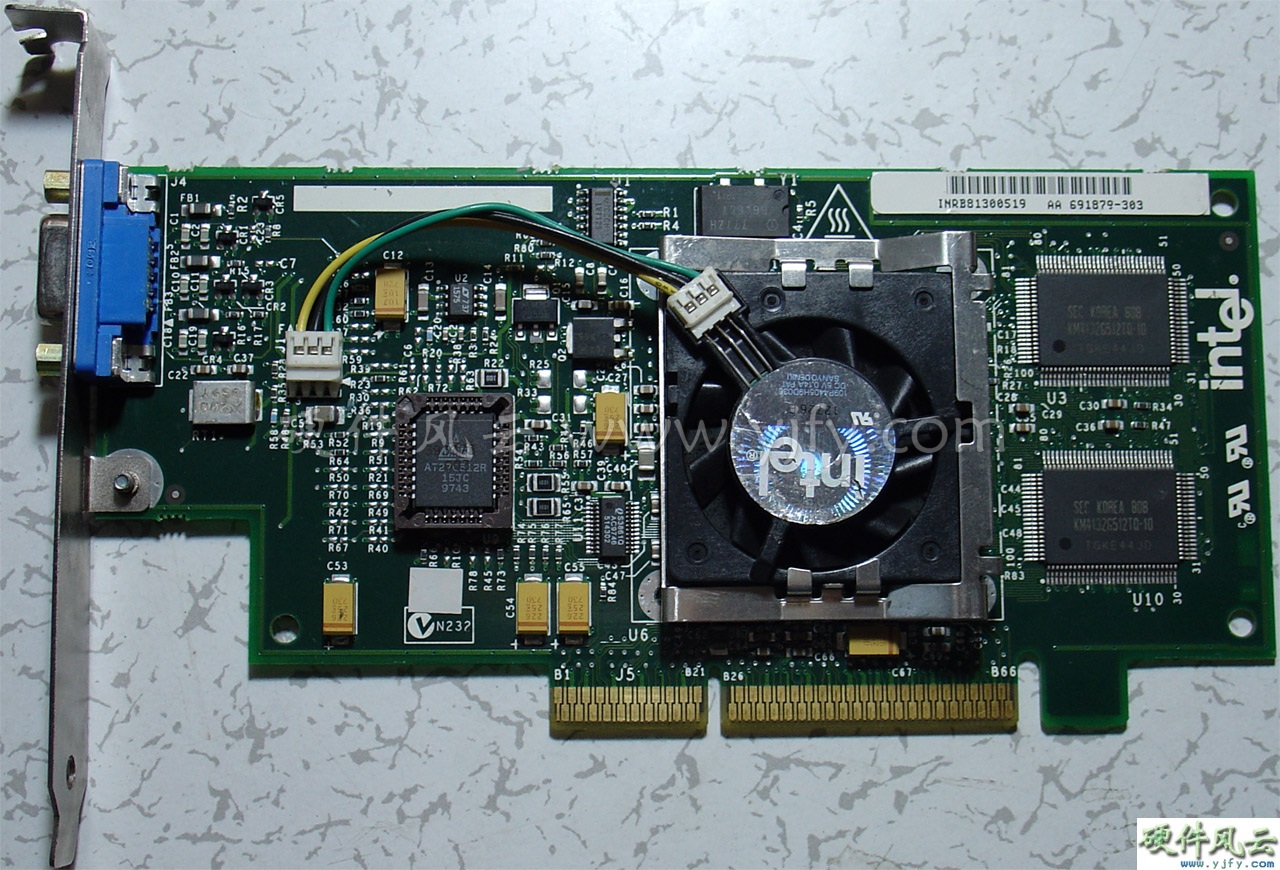
3.2.5.2 Express 3D Test board
This Express 3D graphics card is a Test board that intel completes the
design and is in trial production, which is no different from the
official retail product. Compared with the Express 3D graphics
Evaluation board, you can see obvious changes from the picture: the core
version of the graphics card is upgraded, the BIOS version is updated
from the 002 version to the 003 version that is consistent with the
official product, and the failed certification is reduced from four to
two. The two vertical rows of resistors under the fan interface change
from full to full soldering. Also, the date of this card PCB is 98 years
and 09 weeks, and the official release date of Express 3D graphics card
is April 15, 1998, which is equivalent to 15 weeks in 1998. The test for
the media evaluation agency is mainly the Test board before the release
date.
Express 3D Test board
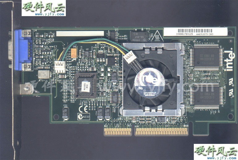
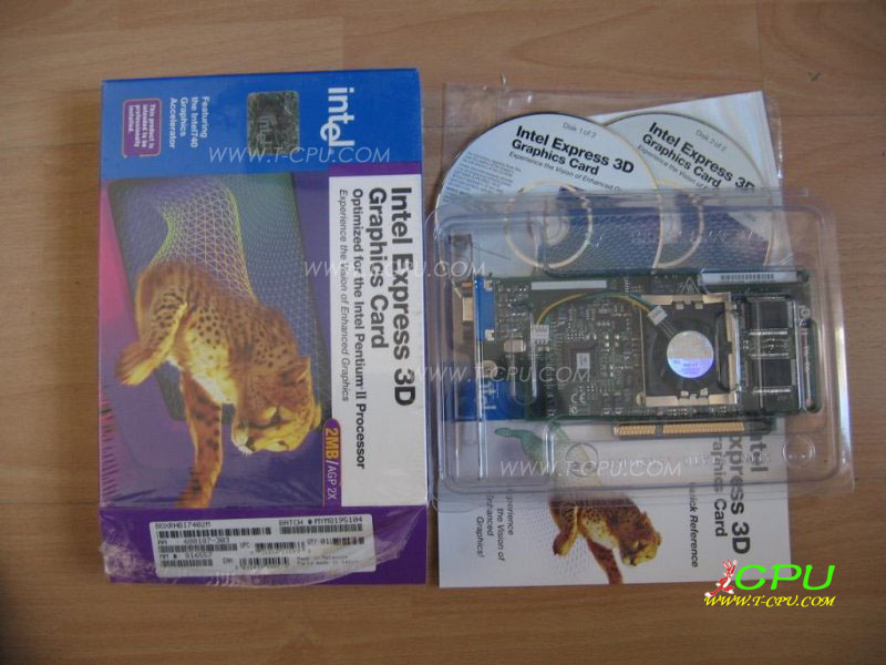
3.2.5.3 Express 3D SGRAM
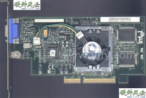
The first civilian-grade graphics card with fan cooling.
Express 3D Qualified Product
The shrink film of the Express 3D graphics card has an intel logo, as if
opening the box would destroy its integrity. Take a look at the rabbit
brother's collection.
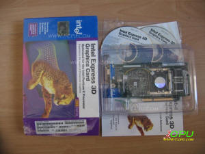
(Source: t-cpu.com)
Compared to the ACTIONMEDIA 750, the box of the Express 3D graphics card
is really too small.

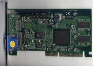
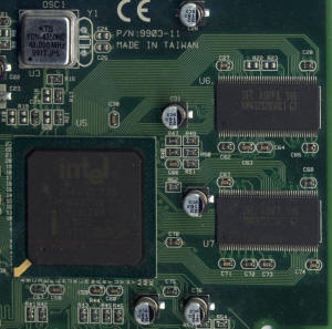
3.2.5.4 Express 3D SDRAM
Express 3D SDRAM memory version.
Express 3D SDRAM Qualified Product

3.3 i752 chip series graphics card
On April 27, 1999, Intel released i752 (codename: Portola) and i754
(codename: Coloma). The i752 uses a 128Bit graphics core with a core
frequency of 100MHz and a maximum memory support of 133MHz and a maximum
of 16MB. The pixel fill rate is 100M Pixels/s, the triangle generation
speed is 3.3M Trianglws/s, and the built-in 250MHz RAMDAC. It adopts
dual pixel pipeline to support environmental atomization, single-cycle
texture synthesis, 16-bit Z-buffer, bump map, texture compression and
other technologies. In addition, it has improved graphics acceleration
performance that can be accelerated for various graphics streaming
formats at the time. The difference between the two chips is that one
supports AGP2× and one supports AGP4×.
I752 and i754, this is just an improved product of the i740 with limited
performance. The i752 chip shipments are limited, and only a small
number of graphics cards have been produced by Gainward. The i754 chip
project was withdrawn.
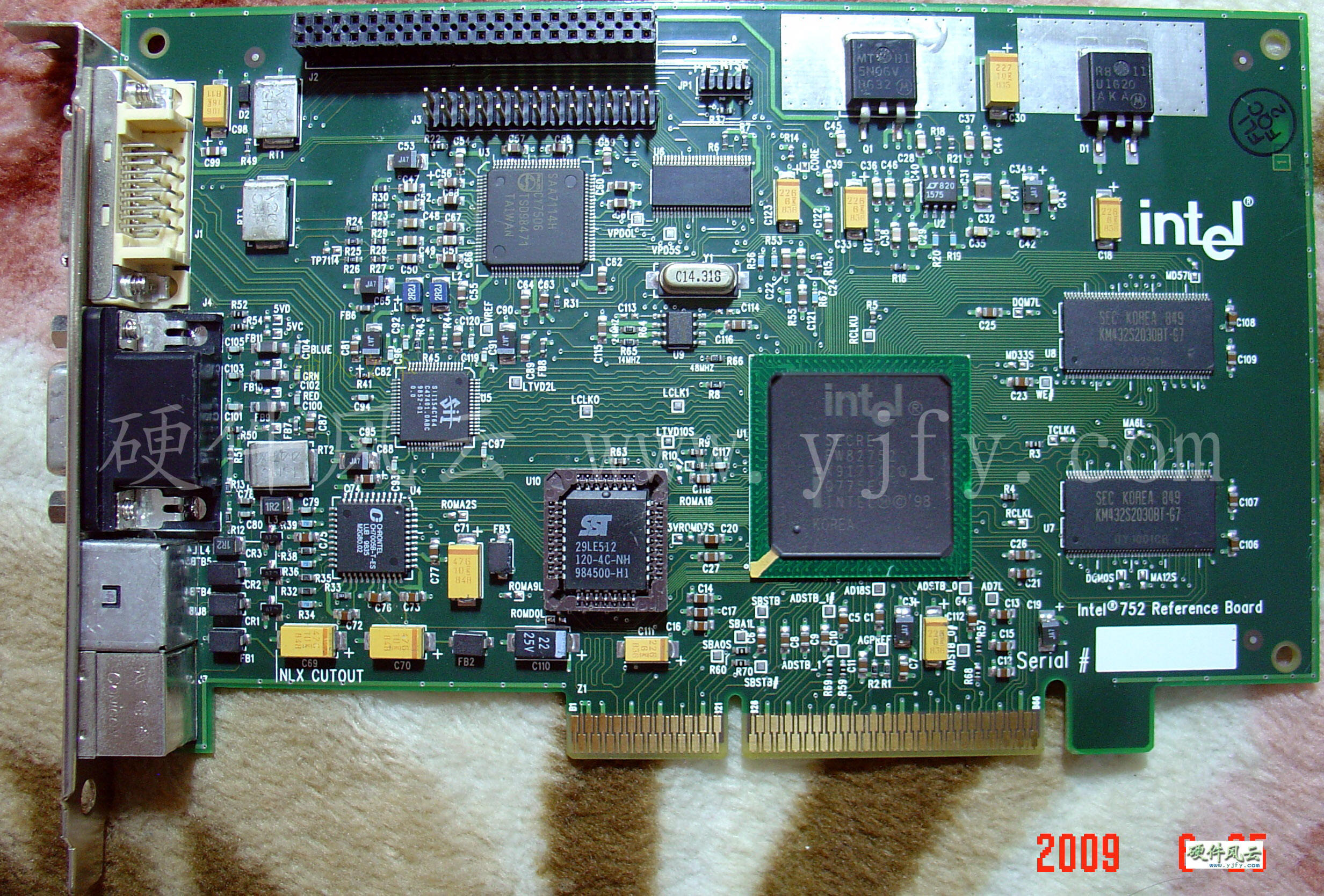
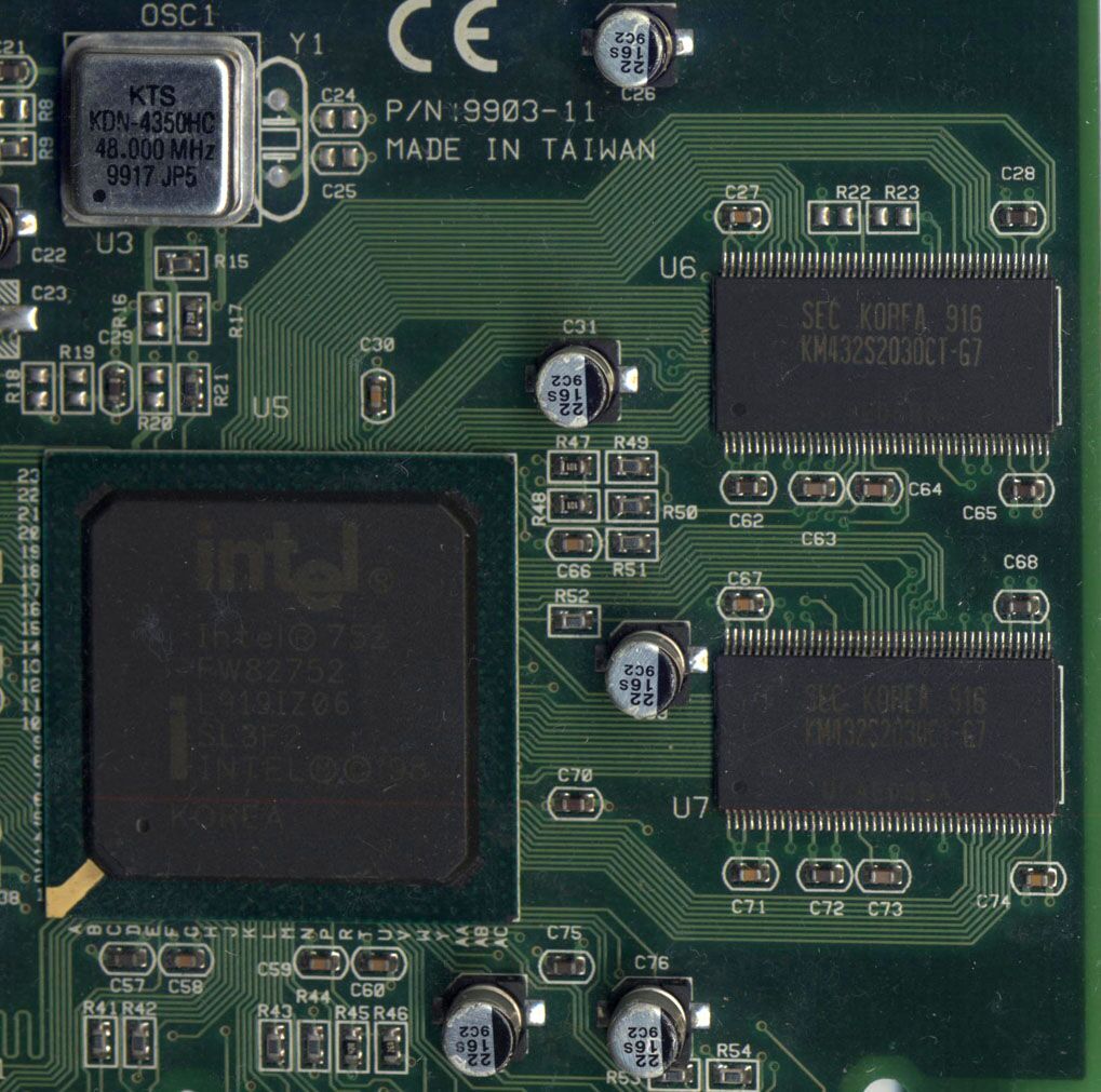
3.3.1 Intel752 Reference board
The display chip date of this i752 reference board is 9917.
Intel752 Reference board

3.3.2 Gainward i752 commemorative card
At Computex 99, intel sent the i752 graphics card to 50 lucky
viewers, which is the Gainward i752. The only symbolic sale of the i752
chip graphics card. After reading the following pictures, you will
understand why intel does not sell i752 chips.
Gainward i752 commemorative card
i752 Chip
The
i752 chip above is a formal chip with a date of 9919.
i752 chip engineering sample

The above picture is a sample version of the i752 chip project submitted
by friend NEST, dated at 9920, later than the official version of the
Gengyu i752 commemorative card, 9919. It shows that the official version
of the chip is not perfect, there are many problems, just intel in order
not to jump the ticket, only to sell a very small number of i752
official chips. Because Intel has no energy to solve the problem after
it becomes a graphics card, why? And listen to the next decomposition.
|
|
4. 20 years of growing(1999-present)
The I740 chip graphics card is undoubtedly more successful, but
it is at the low end in the graphics card market. At this time, the
3D graphics card market is full of smoke, INTEL enters the 3D
graphics card market by buying and buying, Intel technology
deposition is limited, technology integration, innovation takes
time, can only find another way.
On February 20, 1997, Cyrix launched the Media GX chip of the IT
industry's first chip integration solution (All in One). This
epoch-making concept, "Integration," was later understood by Intel
and introduced an "Integrated Graphics" solution in early 1999. On
April 26, the i810 chipset with integrated i740 display core was
released. The i810 has achieved unprecedented success in the market
and has contributed greatly to the popularity of integrated
chipsets.
4.1 Integrated Graphics
The i740 and i752 display cores are integrated into the north
bridge chip of the i810/815 motherboard chipset, which shows that
the core occupies part of the main memory of the computer during
operation, which reduces the performance of the computer, but the
cost and power consumption of the entire platform is lower.
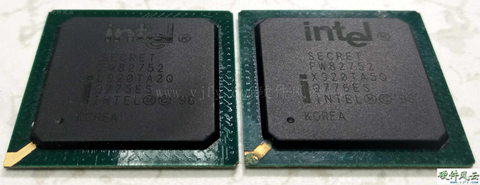
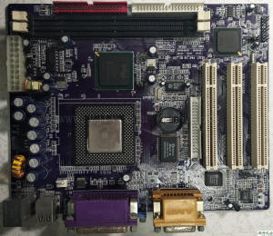
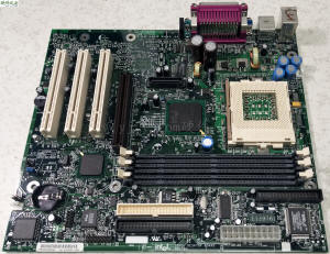
4.1.1 i810 Series
The question about whether the i810 integrates the i740 or the
i752 display core has been debated. The display chip date of the
i752 reference board in this paper is 9817, and the date of the i810
North Bridge chip integrated with the display core on the CA810
motherboard is 9816. It is impossible for the i810 chip to integrate
the i752 display core, which is also in the engineering sample
stage, and should be the i740 display core.
The i810 series has i810, i810E and i810E2.
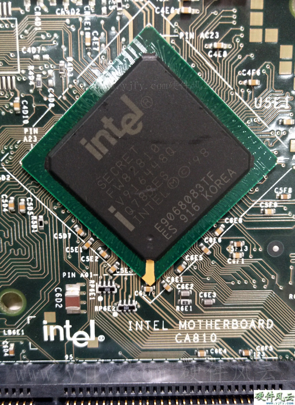
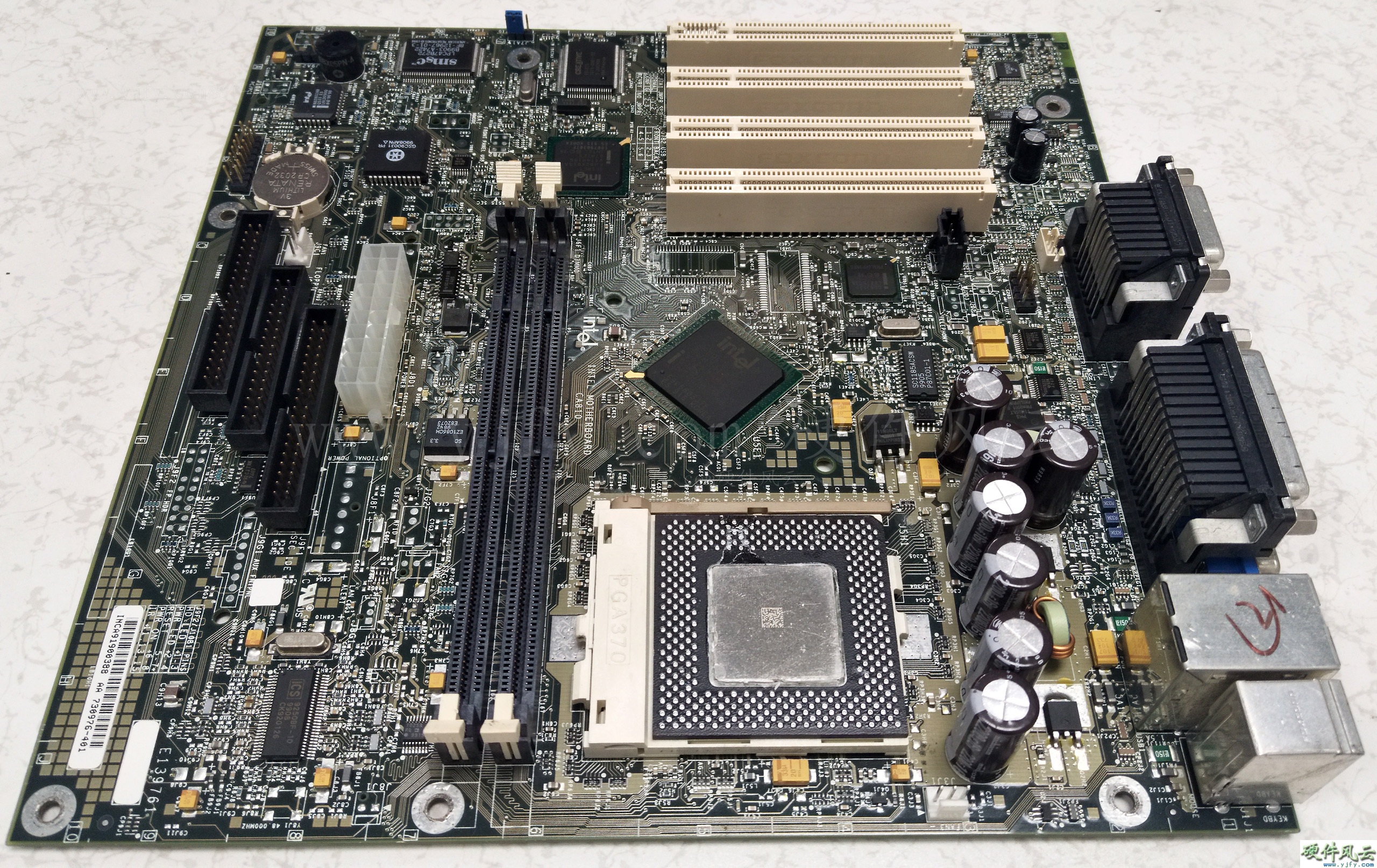
4.1.1.1 i810Chip
The i810 chip was released on April 26, 1998, and the first
cluster display board CA810 was released on June 25.
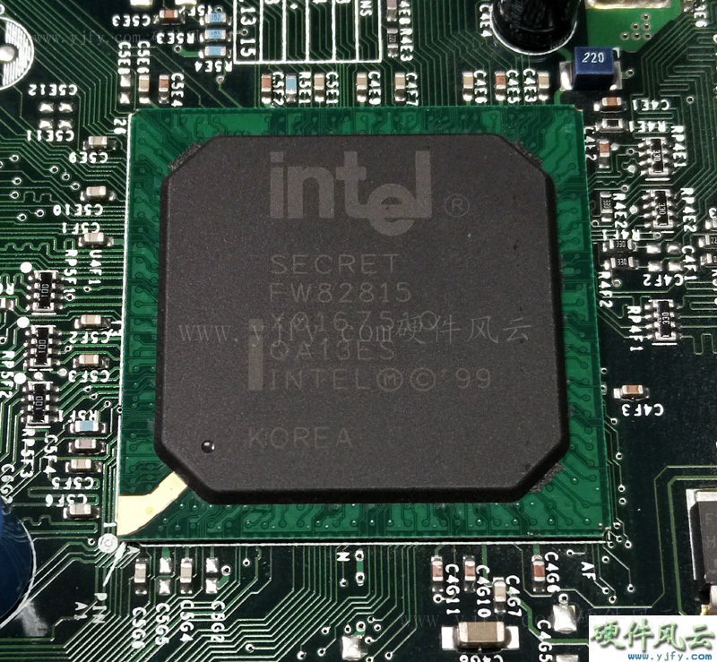
i810 chip engineering sample
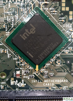
CA810 Mainboard Engineering Sample

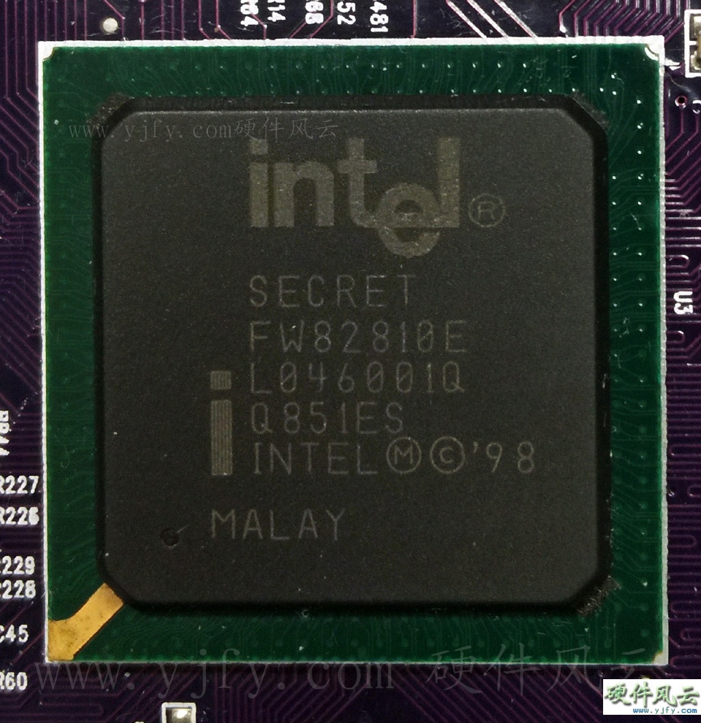
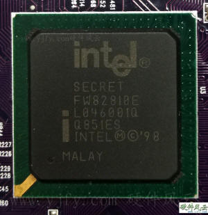
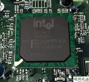
4.1.1.2 i810EChip
Released on September 27, 1998. The difference between the i810E
chip and the i810 chip is to support the 133MHZ FSB.
his unknown brand-name motherboard uses a rare i810E engineering
sample chip.
i810E chip engineering sample
4.1.2 i815 Series
The i815 chip has built-in i752 display chip and adds digital
video signal output port (DVOP). There are four kinds of i815,
i815E, i815G and i815EG.
4.1.2.1 i815 Chip
Released on June 19, 2000, the display core is the final result
of the i752 graphics card project.
i815 chip engineering sample
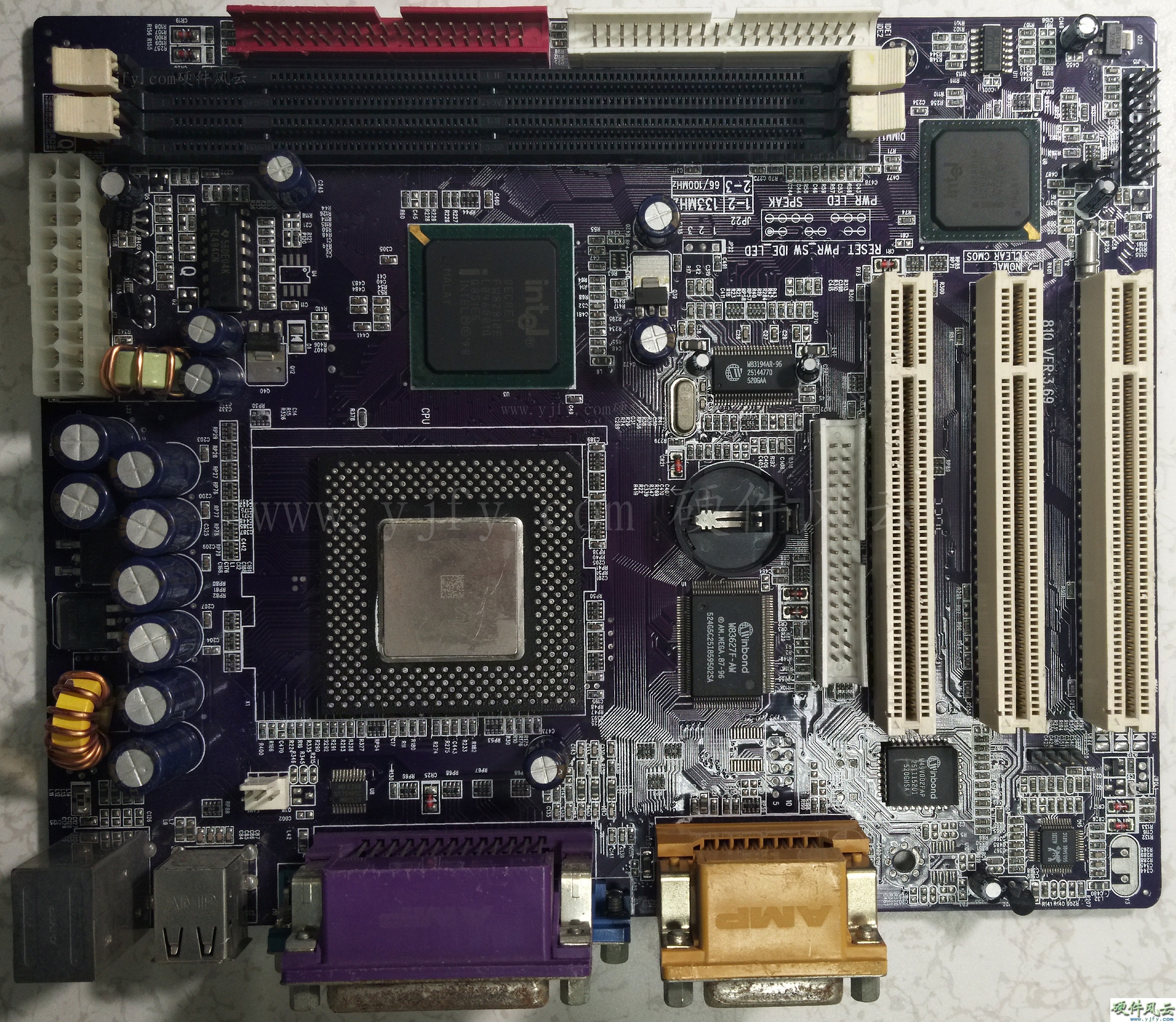
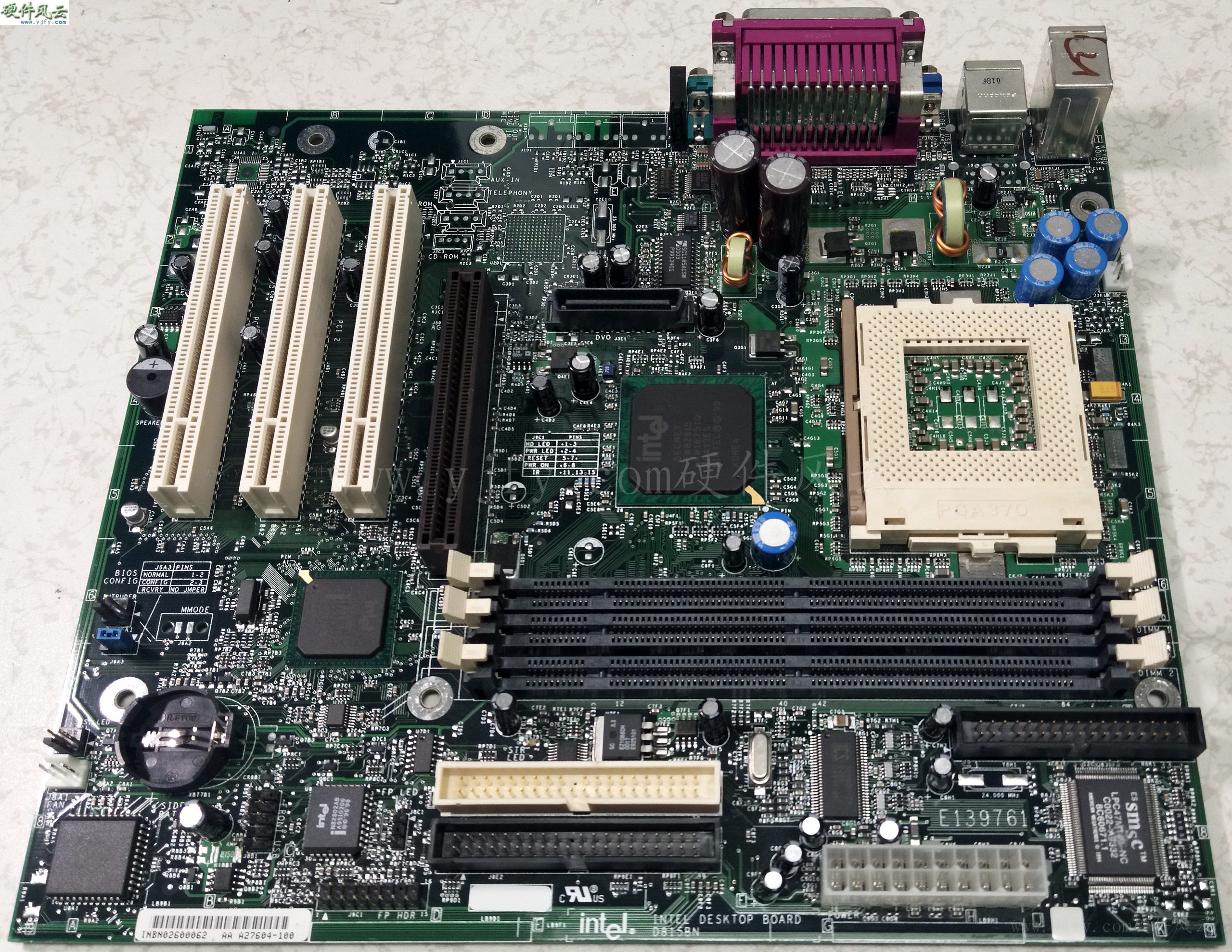
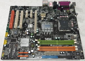
D815BN Mainboard Engineering Sample
4.1.2.2 i815 B-STEP Chip
i815 B-STEP is an upgraded version of i815 and supports Pentium III
Tualatin CPU.
i815 B-STEP chip engineering sample
i815 B-STEP chip engineering sample
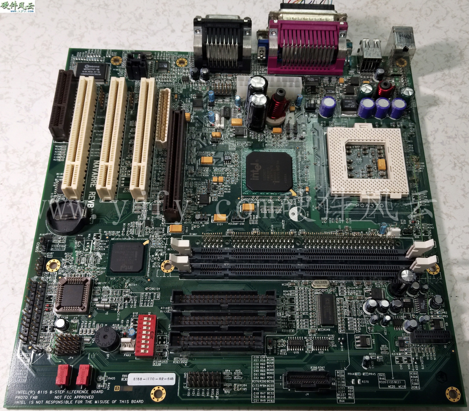
INTEL 8115 B-STEP Reference board

4.1.3 Extreme Graphics Series
In 2002, Intel introduced the i845G/E chipset with integrated
"Extreme Graphics", which has significantly improved performance
compared to the previous generation. The core frequency is 200MHz in
the i845G, and the core frequency is 266MHz in the i845GE. The
performance is close to that of Nvidia. Geforece2 MX 200, Extreme
Graphics supports DVMT technology, which can dynamically call memory
from the system, from the initial call 8MB to call 48MB.Products are
i845G, i845GL, i845GV, i845GE.
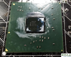
4.1.3.1 i845G
i845GE Chip
The heat
sink on the chip of this motherboard is soldered and cannot be
removed. Only retail i845G chip pictures can be displayed.
i845G Mainboard Engineering Sample

4.1.3.2 ADD expansion card (Advanced digital display)
The ADD expansion card is not a stand-alone device. It must work in
conjunction with the Intel Graphics Memory Controller Hub (GMCH) to
provide high quality digital signal output. It provides an external
graphics processing engine via a 1.5v AGP interface that provides
digital signal output.
Intel's PB C58792-002 ADD card adopts full-height design and supports
DVI/video input and output. It is used in 845G series chipset
motherboard. This card can output integrated graphics to the LCD through
the AGP interface of the motherboard, and add extra Video input and
output functions.
PB C58792-002 Engineering Sample
4.1.4 Extreme Graphics II Series
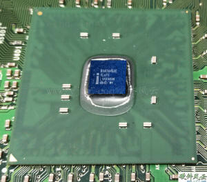
Intel has improved on Extreme Graphics and released Extreme
Graphics II. Products are i865G, i865GV.
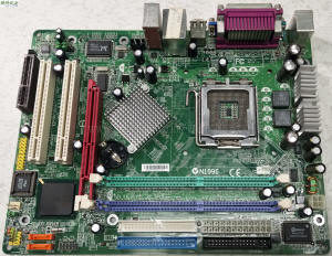
i865GV Chip
MSI MS-7101 Mainboard Engineering Sample
4.1.5 Graphics Media AcceleratorSeries
On June 21, 2004, GMA (Graphics Media Accelerator) Intel graphics
chip was born. GMA is Intel's built-in graphics core product line
from 2004 to 2008. Products are i910, i915, i945 series and so on.
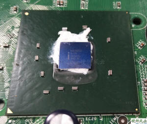
i945 Chip Engineering Sample
MSI MS-7161 Mainboard Engineering Sample
4.2 CPU with integrated graphics
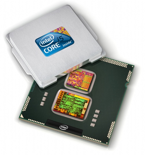
On the afternoon of January 8, 2010, Intel held a new Intel Core
Launch Conference in Beijing. Intel officially released the latest
revolutionary products worldwide, based on the new 32nm process Core
i7, i5, i3 processor products. The Core i5/i3, which uses the Westmere architecture and is code-named Clarkdale, pioneered the
integration of processors. It is the first CPU integrated with a GPU
graphics core. The CPU is integrated with the GPU chip for the first
time.
Here are a few representative Core processors.
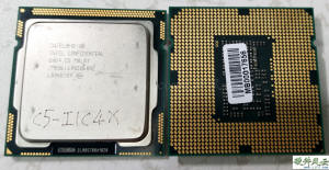
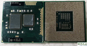
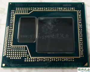
4.2.1 Core 1st generation
The new generation Core i3/i5 processor, code-named Clarkdale, is
packaged on the same substrate as the CPU. Although the CPU/GPU is
packaged on the same substrate for the first time, the CPU part and
the GPU part are independent. The CPU part adopts the 32nm process,
and the GPU part adopts the 45nm process. The name is changed from
GMA to HD Graphic's GPU core frequency. At 733MHz, performance is up
to 50% higher than the previous generation GMA X4500HD. Although
Clarkdale has not yet fully integrated the two cores of CPU and GPU,
it is already a big breakthrough.

(Image
courtesy of http://www.expreview.com)
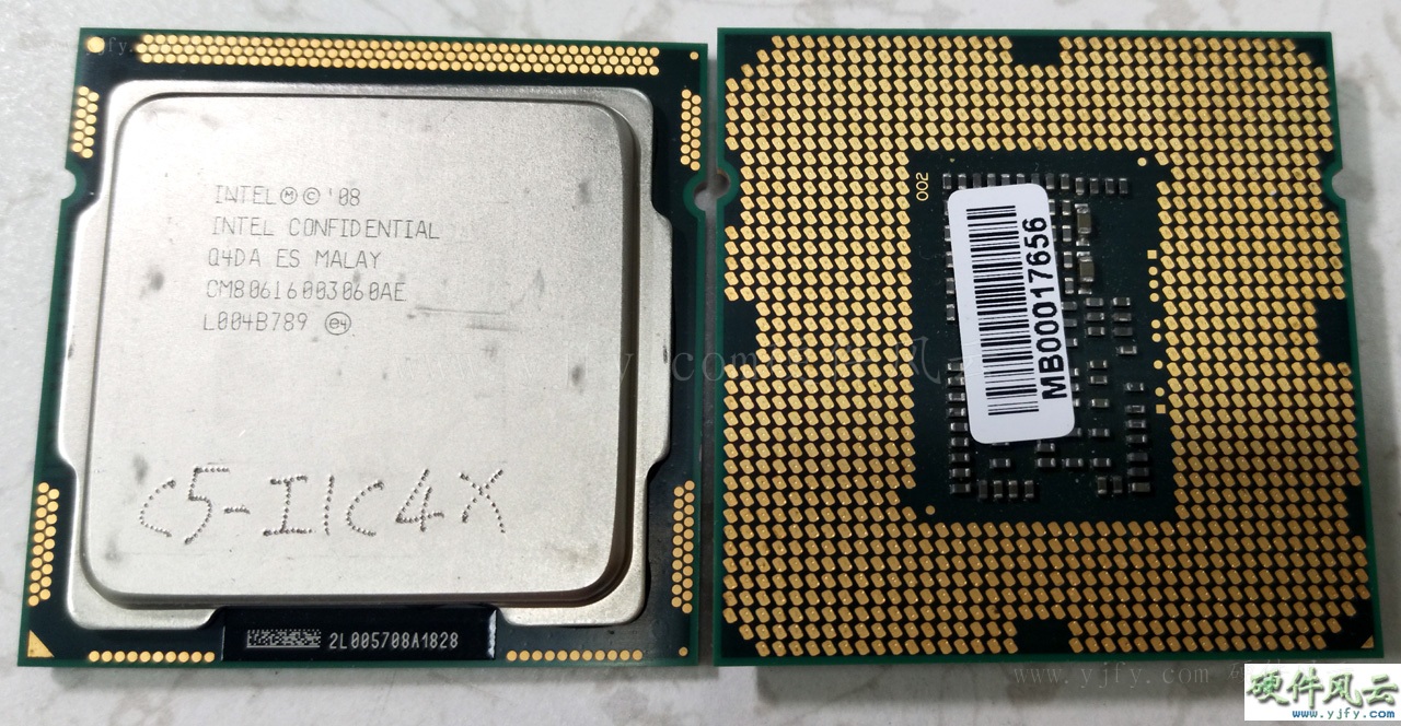
Core i3 Desktop version engineering sample
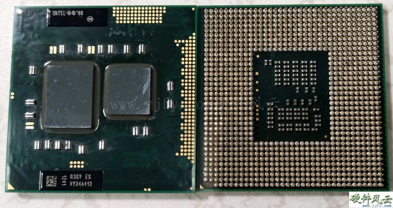
Core i3 mobile version Engineering sample
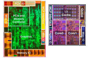
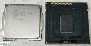
4.2.2 Core 2nd generation
In January 2011, Intel released a new Sandy Bridge architecture,
which first merged the GPU chip with the CPU, and the built-in
graphics core was upgraded to HD Graphics 2000/3000. There are 6 and
12 EU programmable shaders respectively.
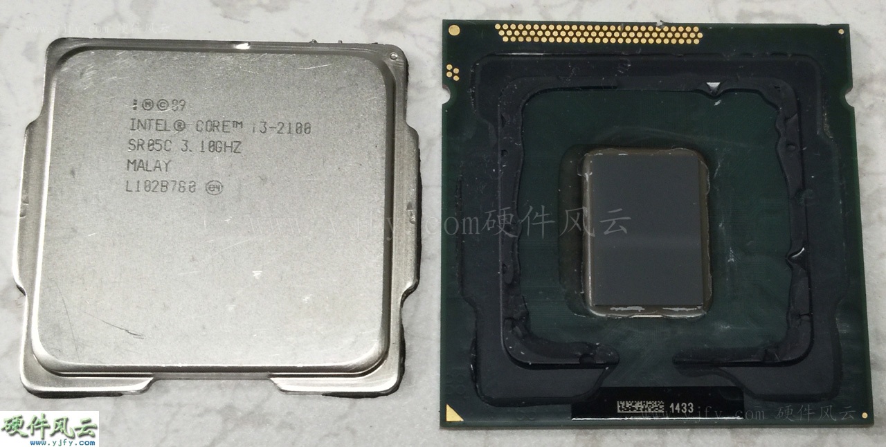
Opened Core i3 2100
4.2.3 Core 4th generation
Core 4th generation enhances display performance. Added eDRAM
memory, supports 4K x 2K resolution, and upgraded high-speed video
synchronization technology to make graphics images decode faster.
The Intel HD Graphics 5200, codenamed GT3e, is called Iris Pro and
has an eDRAM module that represents the strongest display
performance of this generation.
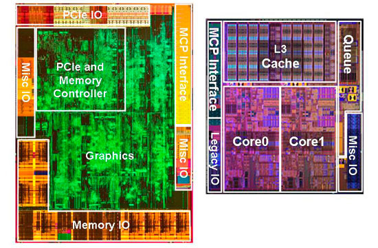
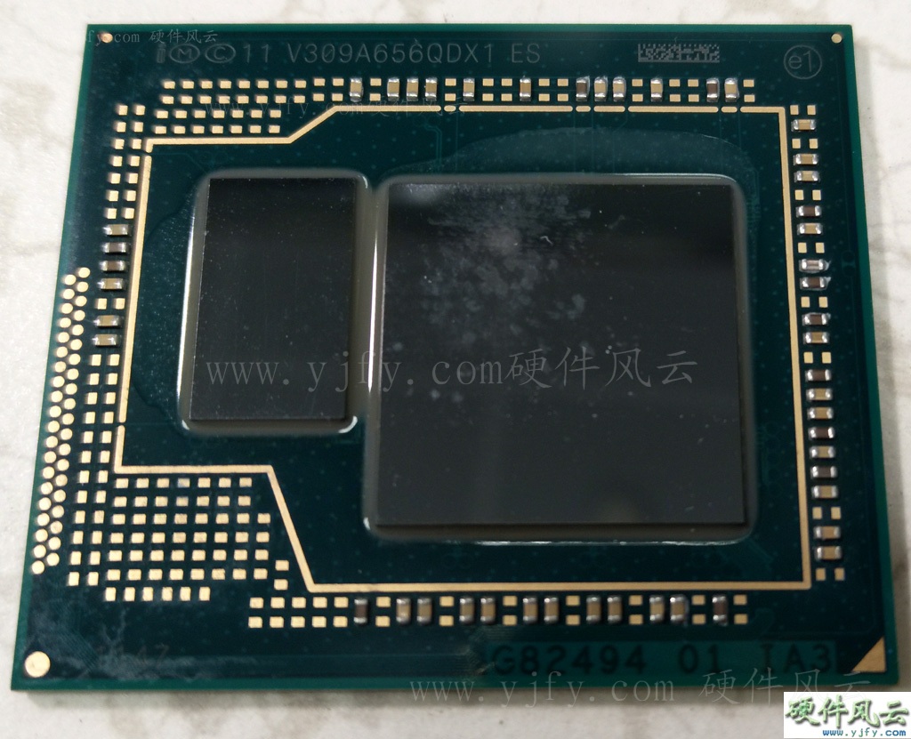
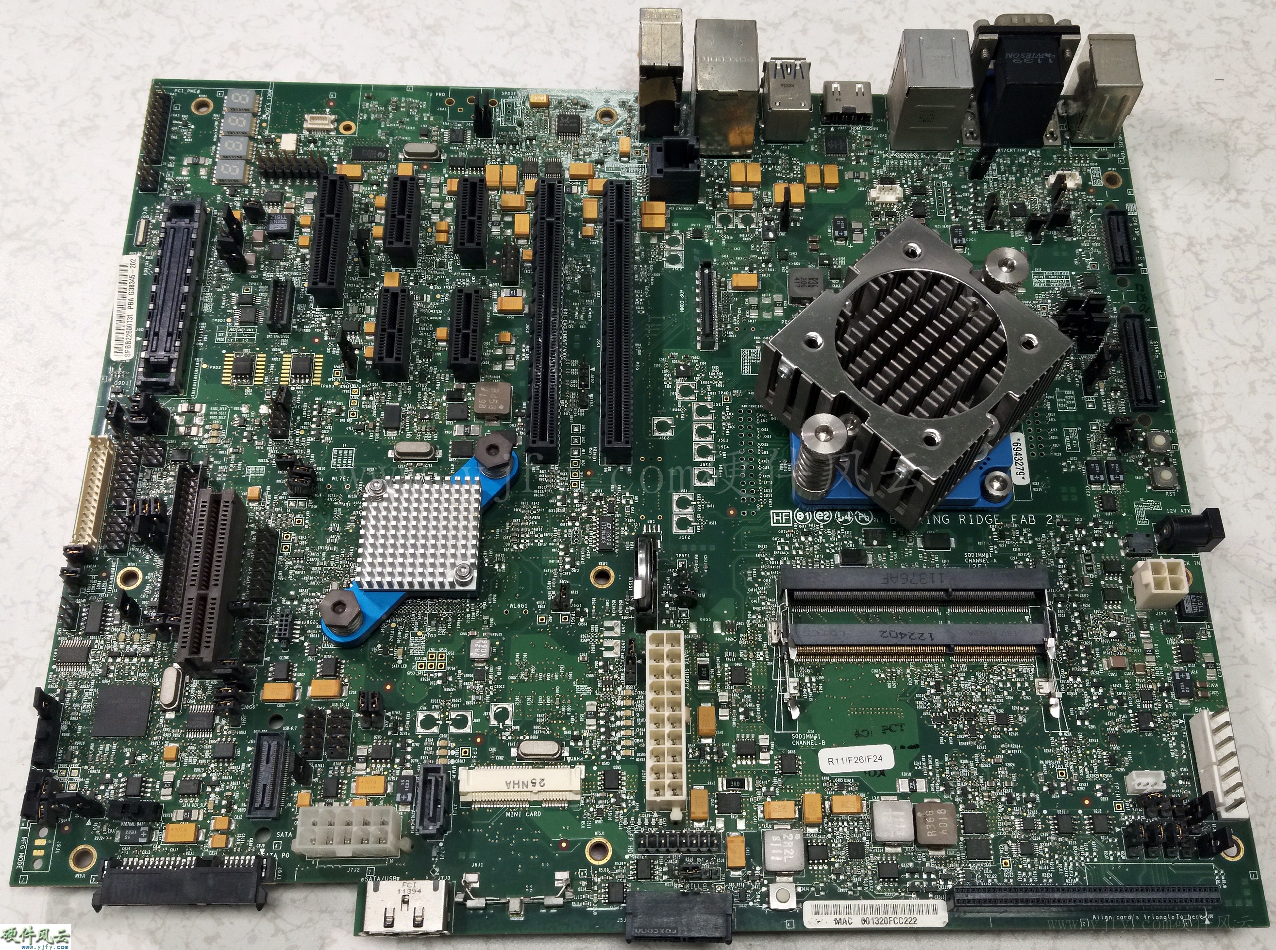
On the fourth generation of Core processor CPU board, there are
two cores, the small core is eDRAM memory. From this Core CPU board,
the CPU core is no longer monotonous, and there will always be other
cores.
4.3
Larrabee
Intel's third-generation discrete graphics Larrabee was first
announced at SIGGRAPH in 2008. Larrabee intends to build a
stand-alone GPU and GPGPU using the x86 instruction set. It was
originally expected that “Larrabee” will be launched in the third
quarter of 2008 and officially released in 2009, but in fact there
were engineering samples in 2009.
In June 2009, Intel claimed that the prototype of Larrabee was
comparable to the NVIDIA Geforce GTX 285. On November 4, 2009, Intel officially announced that Larrabee will
not be released as a consumer GPU product. Instead, it will compete
with Nvidia Tesla as a development platform for graphics and
high-performance computing.On May 31, 2010, Intel completely
canceled the Larrabee graphics card project.
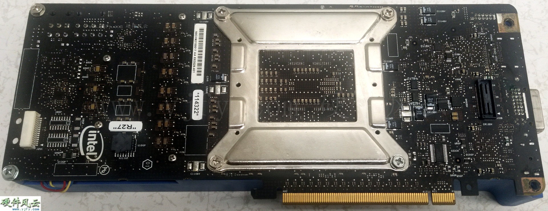
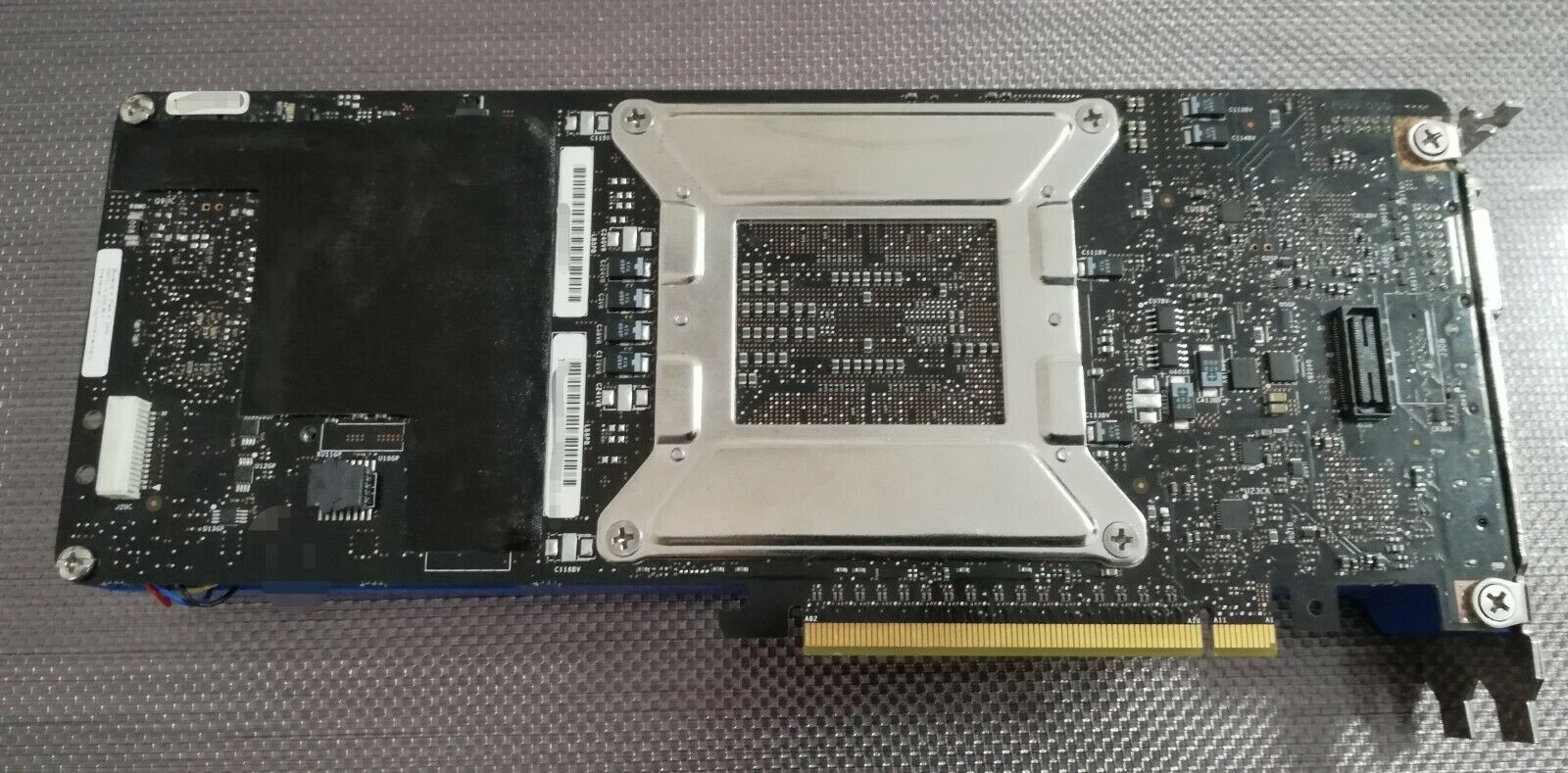
4.3.1 Larrabee
Chip evaluation board
The PCB date of this black PCB version is 0910 weeks.
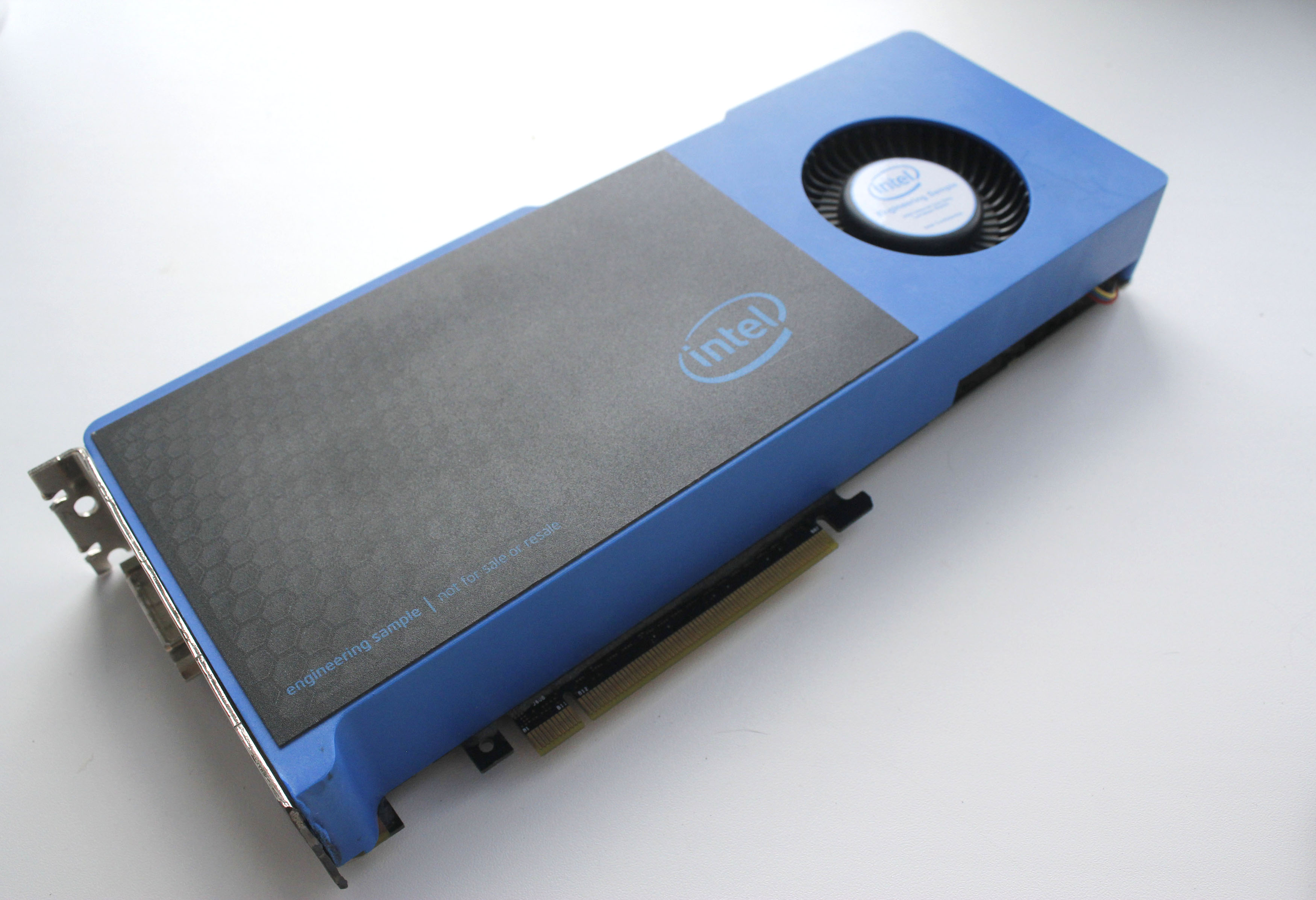
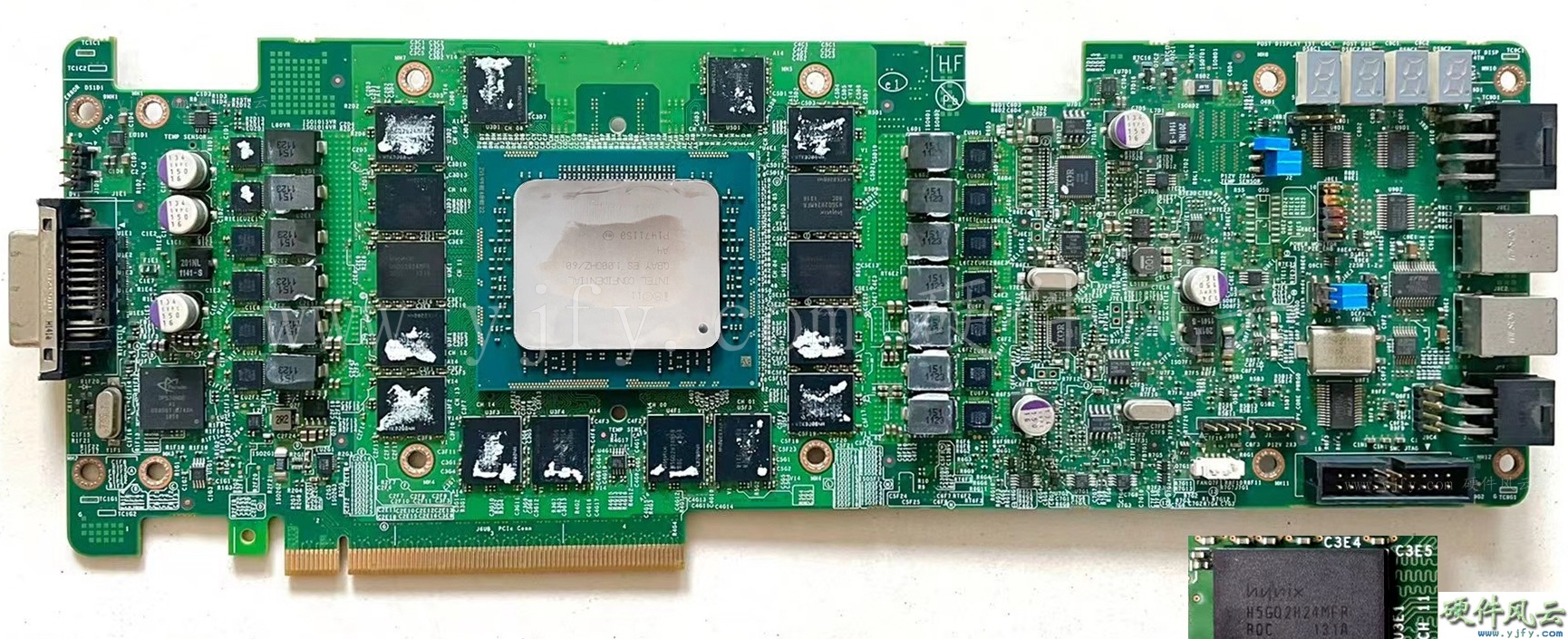
4.3.2
Larrabee
Product evaluation board
The PCB date is 1022 weeks and the GPU date is 1017 weeks.

(From Slaventus86)
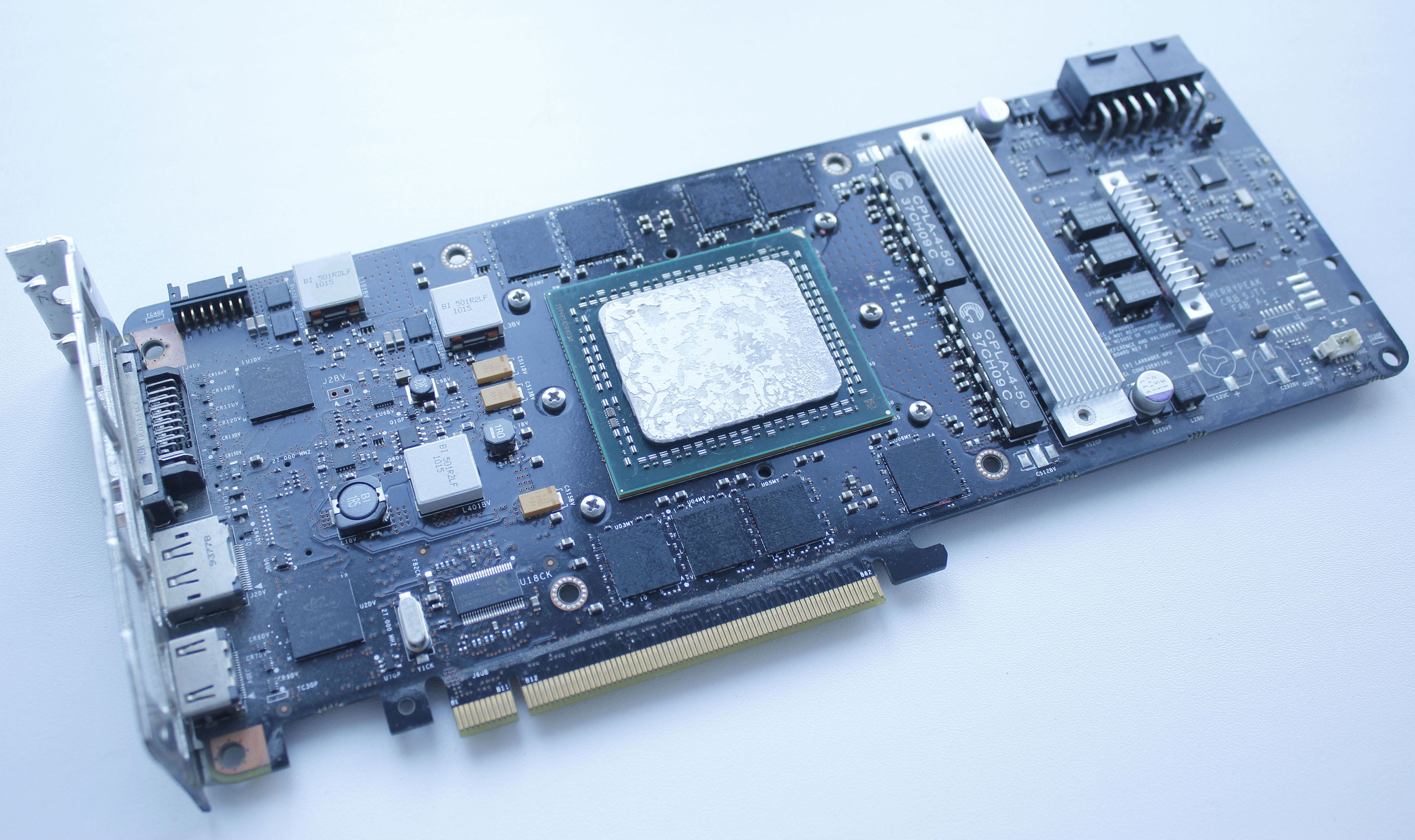
4.3.3 Knights
Ferry
The Rev 3 version is neither marked with "Rev 3" nor "LARRABEE GPU"
on the PCB. It is already Knights Ferry. It can still be called a
Larrabee graphics card because it has a video signal output
interface.
(From leodanmarjod)
Knights
Ferry, which has no video signal output interface, has transformed
from a LARRABEE GPU to a Xeon Phi Coprocessor.
(From PCANG.com)
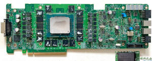
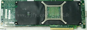
4.3.4 Larrabee2
Knights Corner is an optimization and upgrade of Knights
Ferry. It is only natural that the Larrabee2 graphics card appears,
but Intel did not announce it to the public, and Intel has done such
things.
The PCB date is 3611 weeks and the GPU date is 1147 weeks.
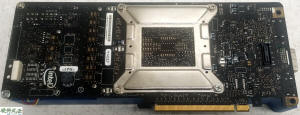
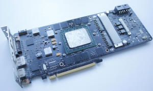
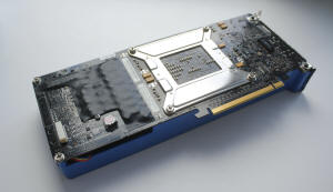
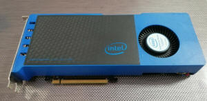
4.4 Unknown
At the beginning of 2018, Intel first revealed the prototype of
the fourth-generation discrete graphics card at the ISSCC 2018
International Solid-State Circuits Conference. The prototype
graphics card was manufactured using the Intel 14nm process and
integrated 1.524 billion transistors.
Where is Intel going, will it open a new era? Wait and see! |
|