|
History of nVIDIA Graphics cards Vol. 1
yjfy |
nVIDIA was founded on April 5, 1993, by Jensen Huang,Chris Malachowsky
and Curtis Priem.
1. NV1
May 22, 1995 nVIDIA Corporation and SGS-THOMSON announced the
introduction of the NV1 and STG2000X Multimedia Accelerators.
The NV1 and STG2000X are the first complete Multimedia Accelerators to
deliver the power of real-time photorealistic 3D graphics, video based
special effects, full-motion video acceleration, and concurrent
high-fidelity audio, in a single chip.
1.1 nVIDIA
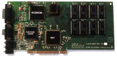
1.1.1 NV1
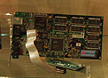
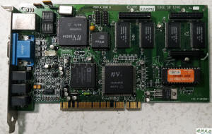
1.1.1.1 Chip Evaluation board
Chip Evaluation board of NV1 graphics card.
(From EDGE magazine Februay 1996)
1.1.1.2 Product Evaluation board
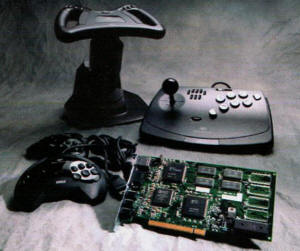
The NV1 graphics card is initially positioned as a 3D game graphics
card, so its Product Evaluation board is naturally related to games and
is equipped with a universal GAME port.
July 31, 1995 Sega and nVIDIA reached an exclusive license agreement.
However, Sega’s gamepads are not compatible with the universal GAME
port. Seeing that there will be a lot of Sega games ported from the
face, nVIDIA designed the Sega game port version.
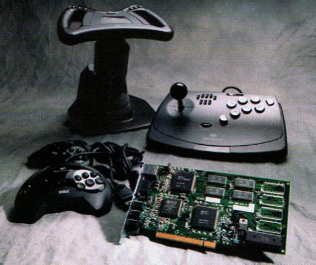
1.1.1.2.1 Game port version
The NV1 graphics card rushes to the bright future of 3D games, and the
official promotional picture theme of its Product Evaluation board is
games.
This Product Evaluation board, 2/4MB VRAM.
(From NEXT Generation Issue #10 October 1995)
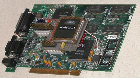
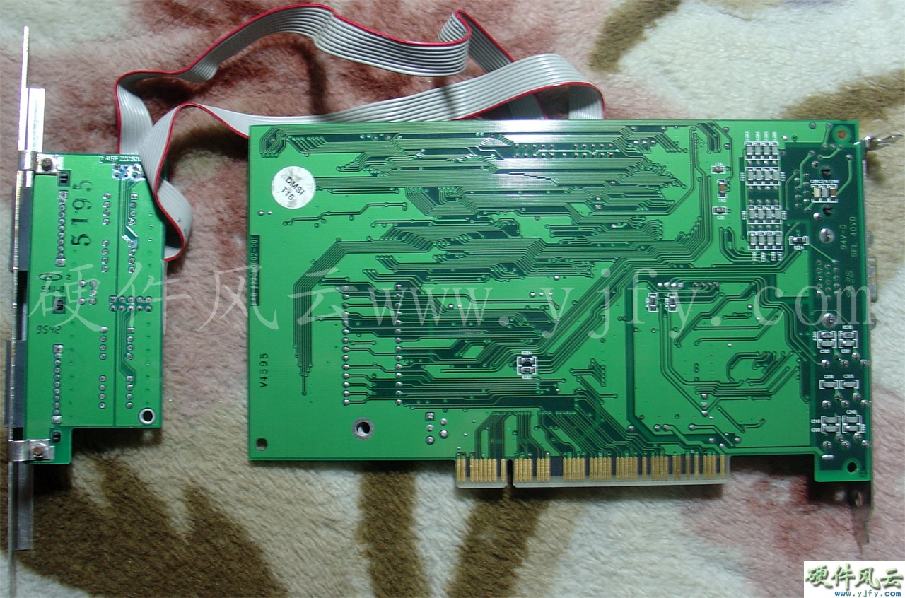
1.1.1.2.2 Sega game port version
This NV1 graphics card is a picture taken by Alexander Medvedev of
ixbtlabs.com in nVIDIA internal museum on 2003.
This version has 4MB VRAM, NVSGP (NV SeGa Port) chip, and an external
game daughter card.
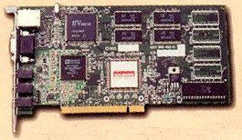
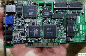
1.1.2 STG2000X
This picture is from anandtech.com and is a collection of Huang Renxun's
office. The ST logo in the picture shows that this is the design of the
STG2000X chip graphics card undertaken by SGS-THOMSON. In fact, the
design work is undertaken by NV. What is interesting is that the chip on
the Chip Evaluation board of STG2000 is not STG2000X but NV1, and the
video memory is DRAM instead of VRAM. This also shows that NV1 chip
supports VRAM/DRAM, STG2000X is only for low-end, artificially limited
to only support 2MB DRAM.
This graphics card is a Chip Evaluation board, not a Product Evaluation
board. The NV1 chip and the NV1 Product Evaluation board have been
basically finalized at this time. With the addition of Sega, nVIDIA
added the NVSGP chip, which was later NVSGP (NV SeGa Port) chip, to
support Sega games handle. Diamond, the first to follow up the pace of
nVIDIA's research and development, has also experienced this situation. |
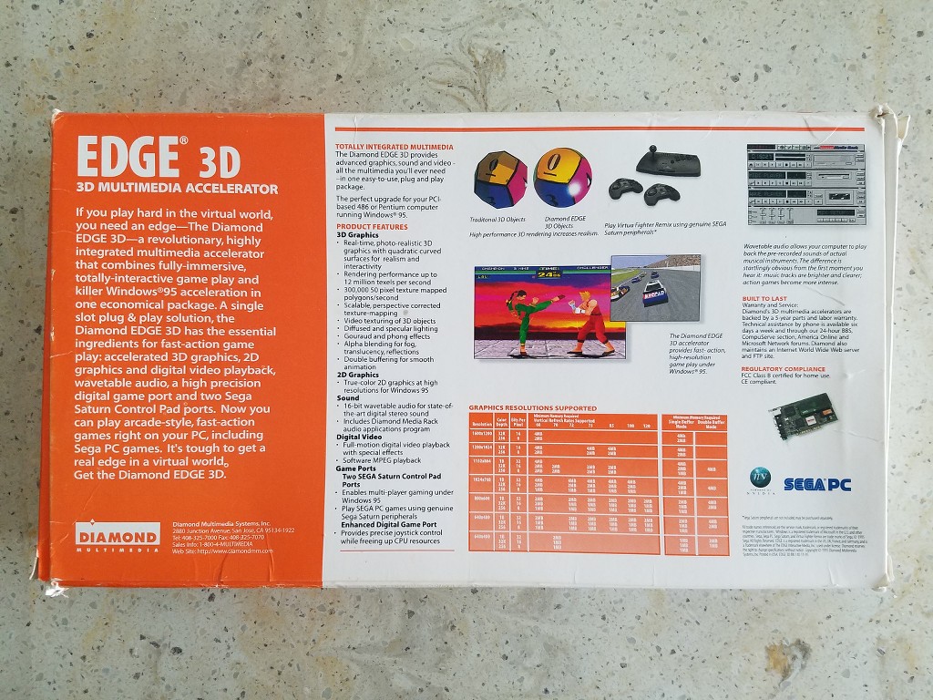
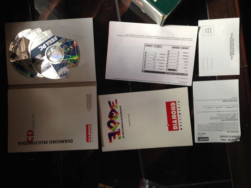
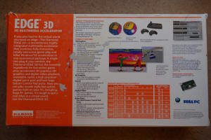
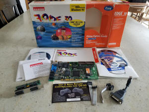
1.2 Diamond Multimedia
May 22, 1995 Diamond Multimedia Systems, Inc. announced its endorsement
of a new generation of Multimedia Accelerators from nVIDIA Corporation
and SGS THOMSON Microelectronics.
November 7,1995 Diamond Multimedia ships Edge3D Series based on nVIDIA
technology.
Diamond is nVIDIA’s earliest and most important partner. Diamond has the
most complete product line based on nVIDIA’s early display chips, the
largest output, and the most representative. This article focuses on
Diamond graphics cards, supplemented by other manufacturers’ distinctive
graphics cards to introduce early nVIDIA chip graphics cards.
In addition, another important reason is that Diamond does not strictly
control engineering samples, and even uses well-functioning engineering
samples directly for OEM or retail. Since most of the engineering
samples are in the early stage of graphics cards, they have an
unparalleled effect on the research of graphics history. There are very
few engineering samples from other manufacturers. Although the main
reason is that the manufacturers destroy almost all of them, our level
of identification is not high enough to distinguish these engineering
samples.
There has been no monograph on the identification of computer board
samples.In the computer hardware collection world at the beginning of
2000, computer collections and CPU collections have become independent
series, and there have been many well-known collectors.Computer parts,
mainly computer boards and cards, are still groping due to their
complexity and variety and the difficulty of collecting them.In the
collection of nearly 20 years, engineering samples have gradually become
the focus of my collection and research.
"Sample
of computer hardware board and card"
is the crystallization of my research results over the years, and plays
an important role in guiding the identification of computer hardware
samples.
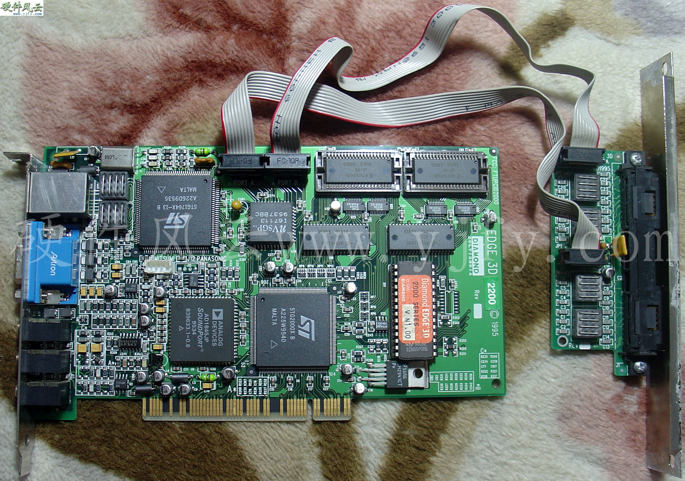
1.2.1 Edge 3D 3000 series (NV1 Chip)
Diamond Edge 3D 3000 series graphics cards use NV1 chips. There are two
models of Edge 3D 3240/3400XL. Edge 3D 3240XL adds a 2MB video memory
daughter card and attaches a green/white "3400" sticker to become Edge3D
3400XL.
In fact, Edge3D 3240/3400XL has two versions. Diamond cooperated with
nVIDIA very early to develop Edge 3D equipped with GAME port version,
and later developed Edge 3D with Sega game port version. This version
with Sega gamepad is the official version.
Because NV1 comes standard with VRAM video memory, the development of
VRAM video memory NV1 graphics card is difficult and costly. Only
Diamond mass-produces VRAM video memory NV1 graphics card. NV1 graphics
cards from other manufacturers are either difficult to produce or use
DRAM version of NV1 graphics cards.
1.2.1.1 Game port version
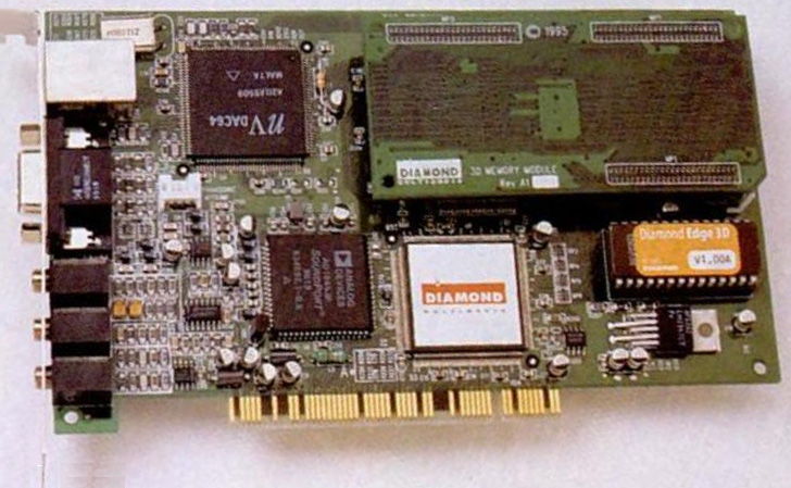
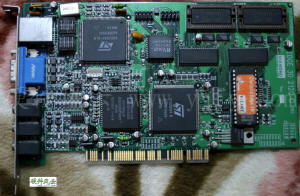
1.2.1.1.1 Early Product Evaluation board
Although this card has the Diamond LOGO, it is not the early Product
Evaluation Board of Diamond, but an engineering sample of nVIDIA. For
the need of publicity, or its Edge 3D graphics card has not yet formed,
or the new product is confidential, it directly affixed its own LOGO to
the nVIDIA graphics card for emergency.
The early Product Evaluation board of Diamond should be the style of the
main daughter card.
(From Computer Gaming World January 1996)
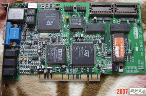
1.2.1.1.2 Late Product Evaluation board
This late Product Evaluation board expands the 2MB VRAM in the form of a
daughter card and has been finalized. Although this graphics card is
quite complete, it is a version that does not support Sega gamepads and
was abandoned.
Note that the graphics card BIOS version is marked as V1.00A.
(From PC Mag on December 5, 1995)
1.2.1.2 Sega game port version
1.2.1.2.1 Qualification Sample
This Edge 3D graphics card is a picture taken by Anand Lal Shimpi of
anandtech.com in Huang Renxun’s office on September 23, 2002.
This Edge 3D graphics card is an Qualification Sample/Customer Sample.
Diamond’s Qualification Sample/Customer Sample graphics cards and some
early graphics cards will have LOGO stickers on the chips, and the
EngineeringSample/Qualification Sample in the official promotional
pictures also have LOGO stickers.
Although this Edge 3D graphics card is Qualification Sample/Customer
Sample, its BIOS version is the official version, marked as V1.00. It
can be seen that there is no letter suffix behind the official BIOS.
(From anandtech.com)
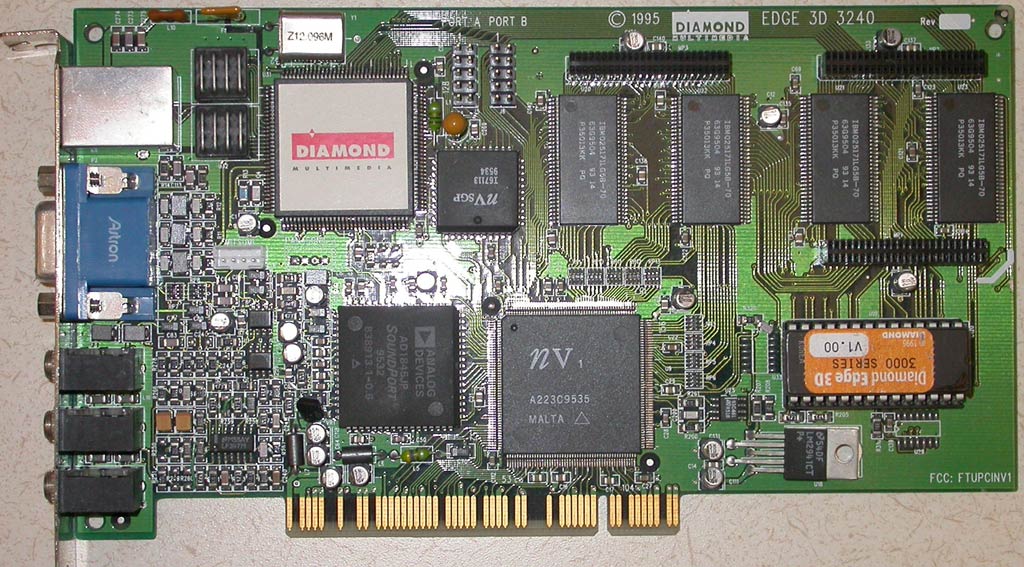
1.2.1.2.2 Official product
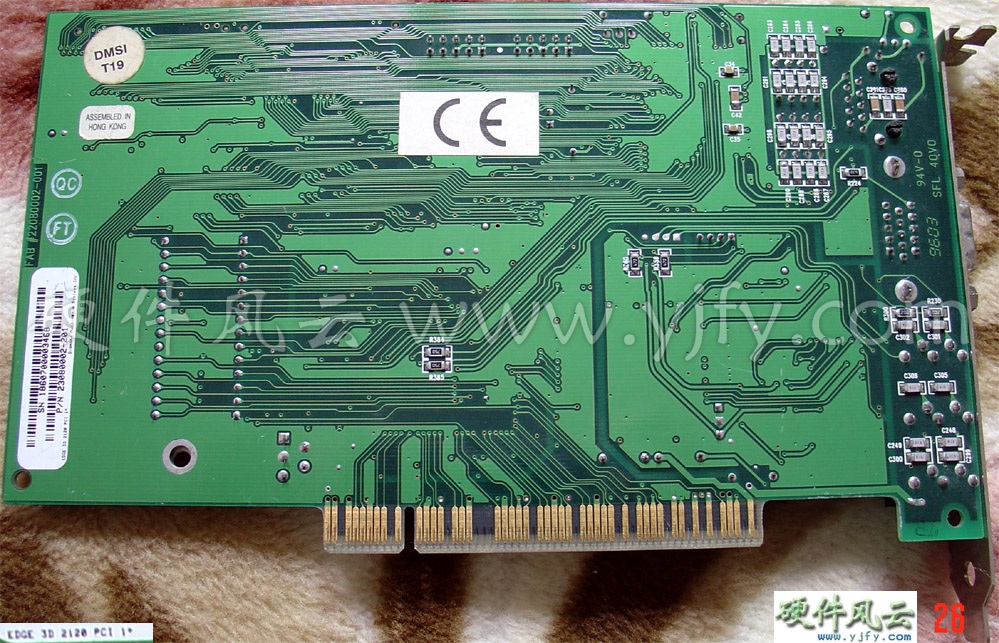
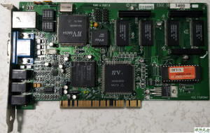
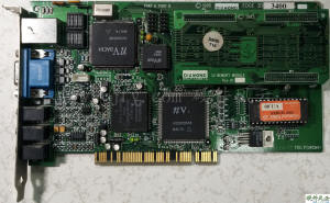
1.2.1.2.2.1 EDGE 3D 3400XL
This graphics card is very similar to the above Qualification Sample.
The NV1 chip and NVSGP chip have the same date, or the EDGE 3D 3000
series early cards all use IBM's VRAM memory and have a white "3400"
label. The PCB date of this graphics card is 9536 weeks, and the
production date stamp is 9543 weeks.
And I have a graphics card with the earliest PCB date of 9534 weeks, but
the chip date used by the graphics card is later than the chip used by
the graphics card at 9536 weeks. The production date stamp is 9547
weeks, 9545 weeks later than the release date.
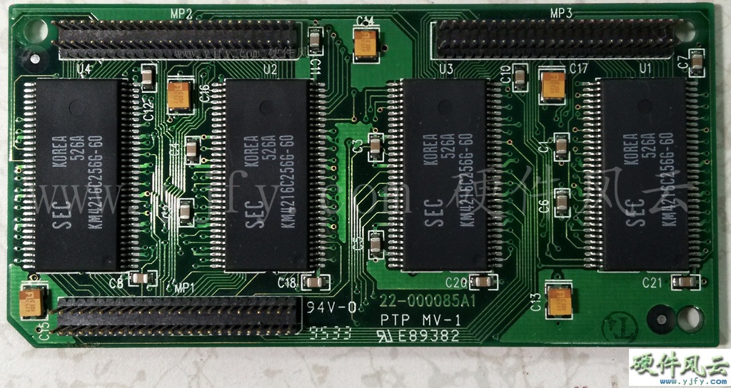
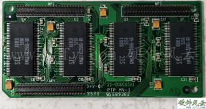
The PCB date of this VRAM video memory daughter card is 9533 weeks,
which can be regarded as an early PCB date. This is because the
video memory daughter card has an earlier finalization date and has
been finalized in the Game port version. The production date stamp
of this daughter card is 9550 weeks.
The later PCB date is 9537 weeks, but it is 9545 weeks. It is
estimated that there are daughter cards that use IBM VRAM video
memory earlier than 9533 weeks.
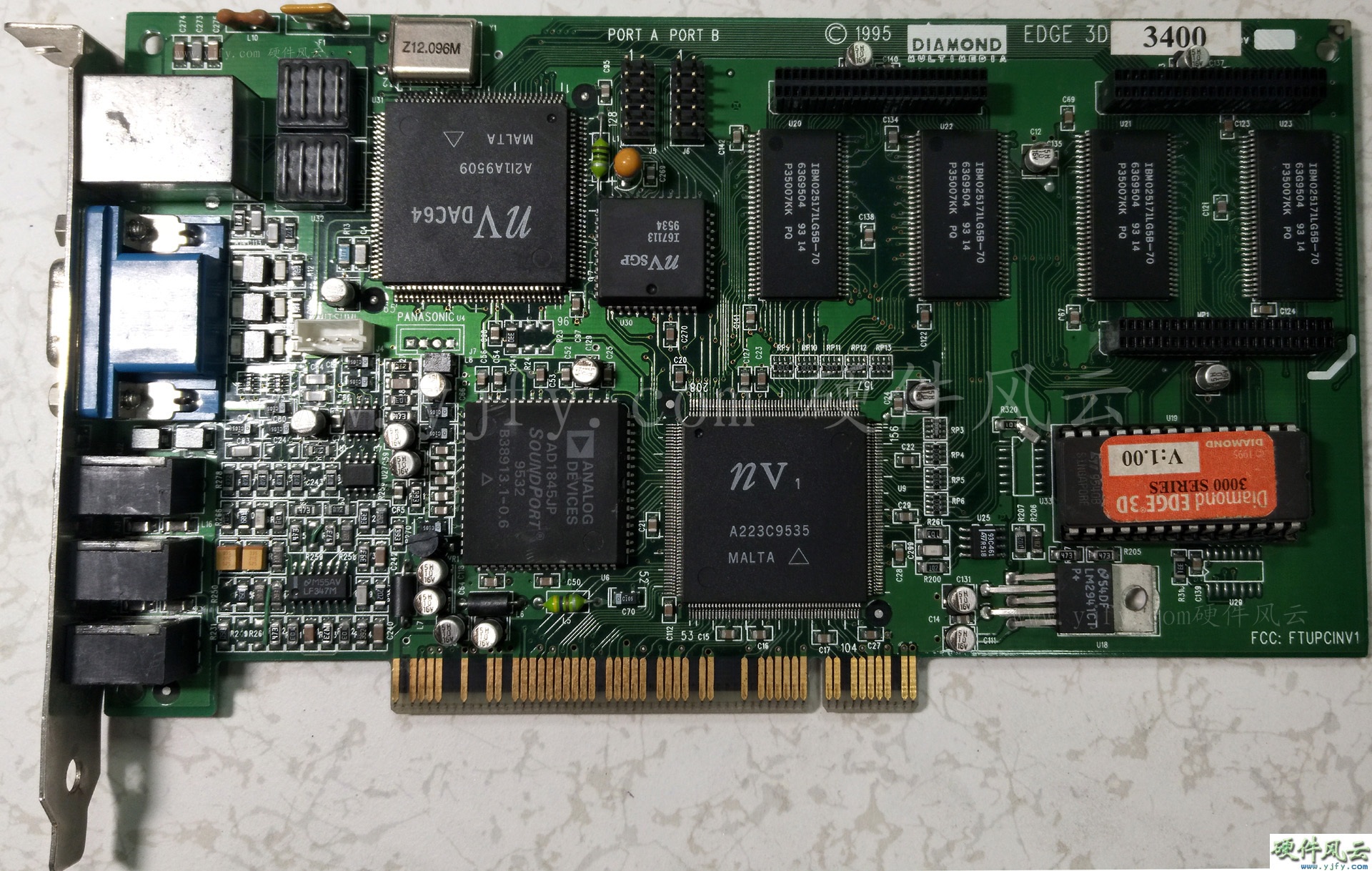
1.2.1.2.2.2 EDGE 3D 3240XL
The NV1 chip is 9531 weeks, the NVSGP chip is 9534 weeks without TM
marking, and the NV DAC64 chip has an earlier date, 9509 weeks, which is
earlier than the date announced by nVIDIA (9521 weeks),Same as the chip
date of the late product evaluation version of the game port version.
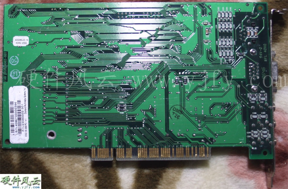
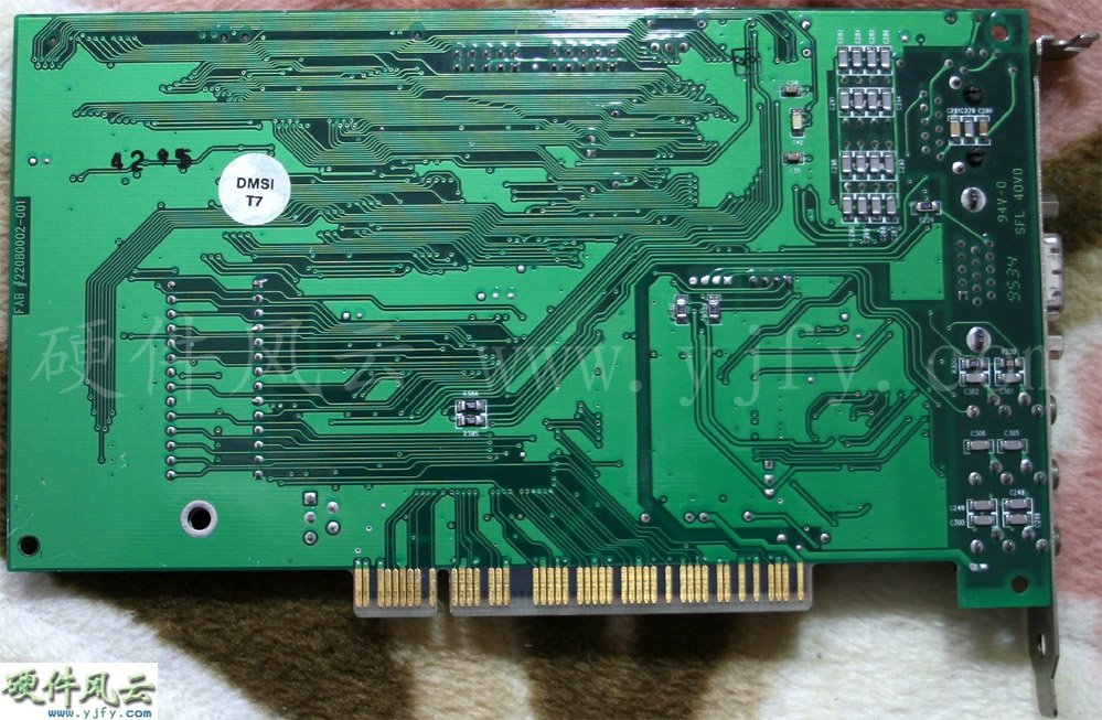
1.2.1.2.2.3 EDGE 3D 2200XL
Some people say that the following EDGE 3D 2200XL graphics card is
fake, because the STG2000X chip is replaced with NV1. In fact, I
found this card from an electronic waste recycling station. This
graphics card appeared late, with a PCB date of 9646 weeks. It is a
chip error graphics card, which also shows that the NV1 chip
supports DRAM. Last year, I bought another EDGE 3D 2200XL on eBay.
Both of its ST chips were replaced by NV chips. The seller also
tested it with the software, but the seller gave a non-existent
postal number and said it was lost. I think it has been collected by
a certain collector and you will see it in the future.

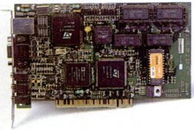
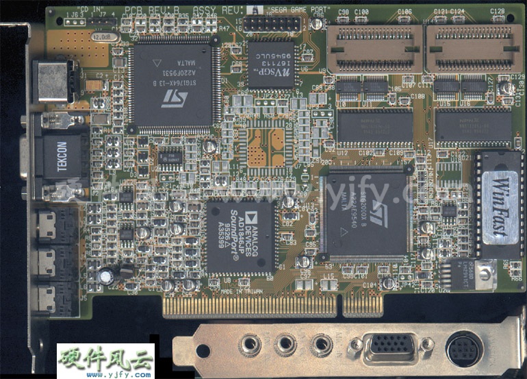
1.2.2 Edge 3D 2000 series (STG2000X Chip)
Diamond Edge 3D 2000 series graphics cards have Edge3D 2120/2200XL,
Edge3D 2120XL can increase 2 slices of 512KB DRAM to expand to 2MB, and
paste the green/white "2200" sticker to become Edge3D 2200XL.
There is no GAME port version for Edge3D 2120/2200XL. It may be that the
STG2000X chip was launched a little later, nVIDIA has cooperated with
Sega, and there is no need to continue to develop the GAME port version.
1.2.2.1 Engineering sample
(From PC Mag on December 5, 1995)
This board type is the late Product Evaluation board. It can be seen
that it is slightly different from the common retail version, and the
obvious change is the position of the aluminum electrolytic capacitor in
the lower right corner of the main chip. The version number of the BIOS
on the graphics card seems to be marked as V1.00C, at least the length
of the handwriting can be judged that there are letters after V1.00,
which also proves that the BIOS of the engineering samples has a letter
suffix.
1.2.2.2 Qualification Sample
Diamond's EDGE 3D 2000 series graphics card saw the earliest PCB
finalization date is also 9534 weeks, and the PCB date of this card is
9534 weeks. The stamp on the back of the graphics card is 9542 weeks,
which means that 9542 weeks is the production date of the card. 11/7/95
(9545weeks) ships Edge3D. This Edge3D 2120XL was produced before the
release date, and the version number on the graphics card BIOS is V
1.00E. It can be seen from the previous EDGE 3D engineering samples that
the BIOS version number of the engineering sample has a letter suffix at
the end, while the official version does not have a letter suffix at the
end.
This graphics card is a sampling of the official product before retail,
and is used in the Qualification Sample for the final test of the BIOS
version. I have bought and sold nearly 100 EDGE 3D graphics cards. Only
the BIOS of this card is special. Although I wrote "Sample
of computer hardware board and card"
, I can only identify this card as the earliest graphics card. Until
this article was written recently, I checked a lot of information to
determine whether it was a sample or a sample of the earliest known
nVIDIA chip graphics card in the hands of collectors.
Why can I collect thousands of engineering samples while other
collectors are hard to find? This is because I have invested a lot of
time, researched in-depth, unique insight, and some elements of luck.

1.2.3.3 Official product
1.2.3.3.1 EDGE 3D 2200XL


The BIOS of this graphics card is VN1.00. "N" should be the meaning of
NEC PC-9821 special edition, this BIOS version of the graphics card does
not display on the PC.
1.2.3.3.2 EDGE 3D 2120XL
1.2.3 Boxed
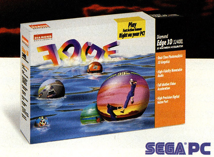
1.2.3.1 Game Port version
This designed box comes from the Diamond website and is the original
design. With the intervention of Sega, it was abandoned. Later, this box
was slightly modified to be used in the NEC dedicated version.
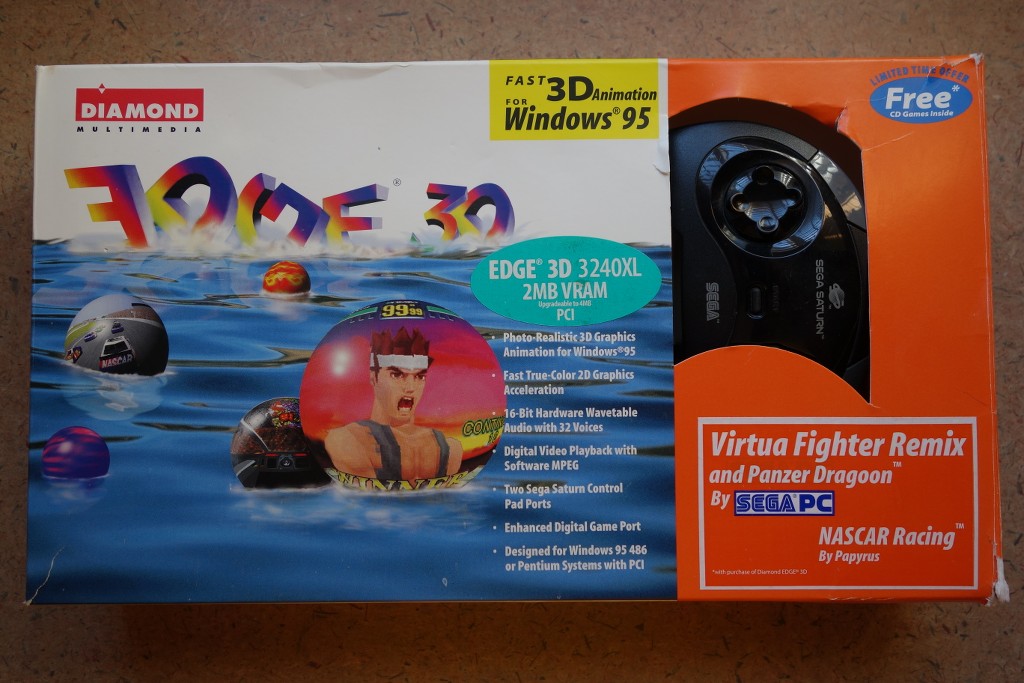
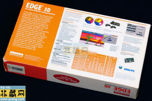
1.2.3.2 Sega game port version
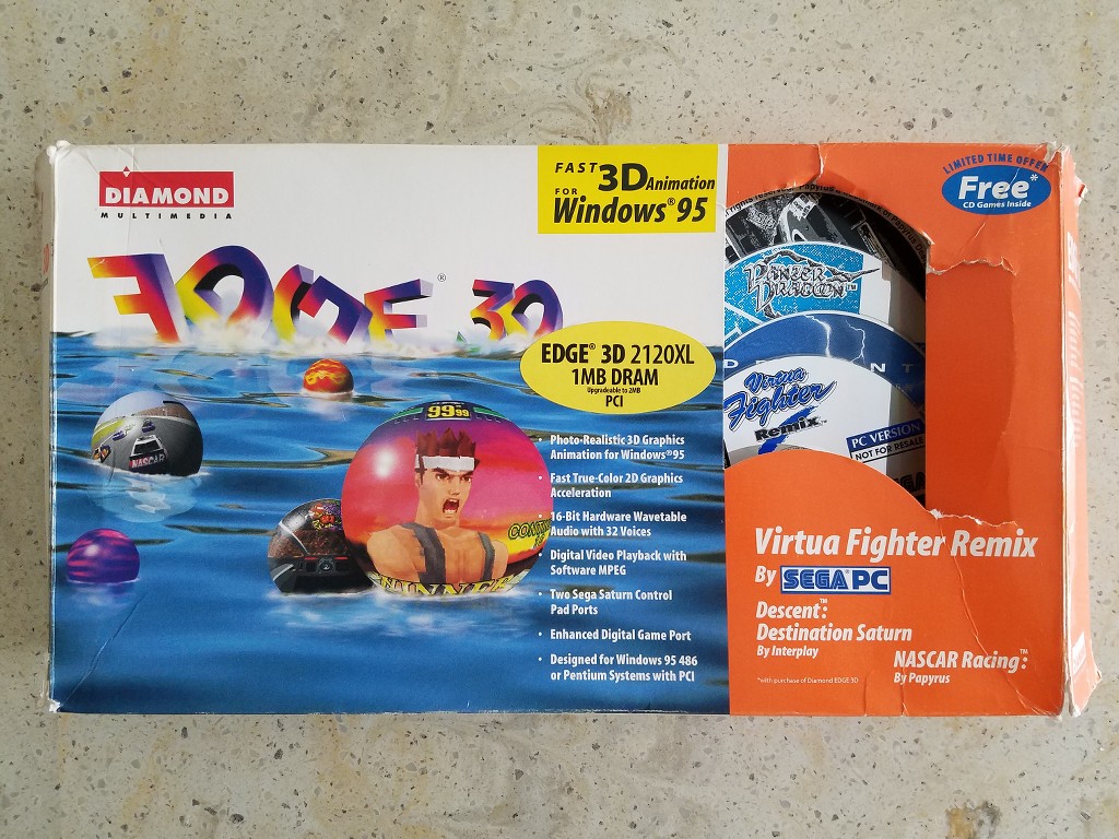
The box of this design is a concept map, and the theme of the box is
Sega Games. It was announced that the EDGE 3D series of graphics cards
will focus on supporting Sega games.

1.2.3.3 Normal version
1.2.3.3.1 Edge 3D 3000 series

(From Artex)
1.2.3.3.2 Edge 3D 2000 series


(From Artex)
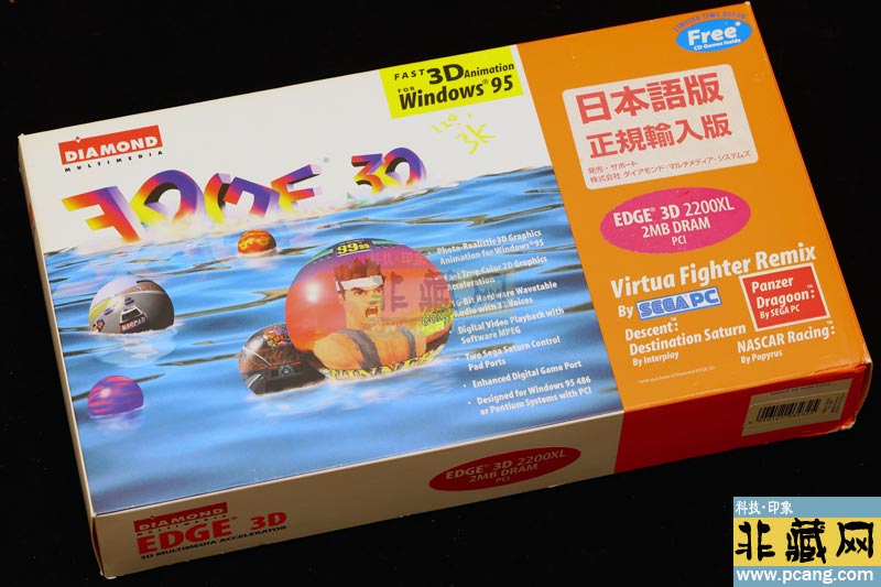
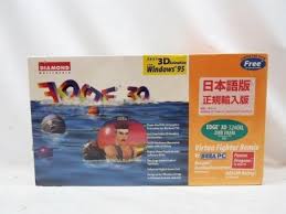
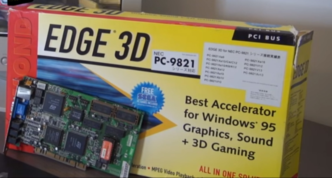
1.2.3.4 Japanese version
1.2.3.4.1 Edge 3D 2000 series

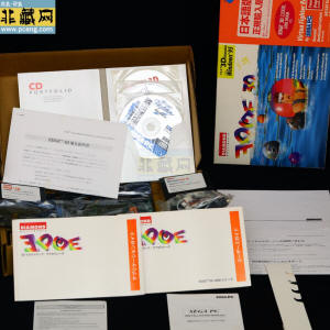
1.2.3.4.1 Edge 3D 3000 series
1.2.3.5 NEC version
(From CompaqGuy youtube.com )
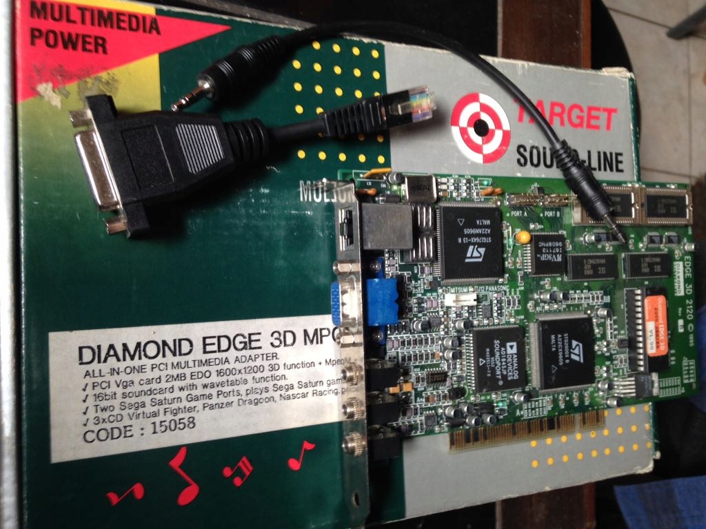
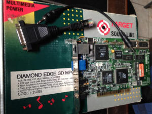
1.2.3.6 TARGET Soundline version
(From allegro.pl) |
1.3 Leadtek Research Inc.
6/01/1995 Leadtek Research Inc. announces Proview GD400 and Proview
GV500.A suggested list price for GD400 at $249 (1MB DRAM) and for GV500
at $399 (2MB VRAM).
1.3.1 Proview GD400 (STG2000X Chip)
Proview GD400 is based on SGS-THOMSON's STG2000 Multimedia Accelerator,
with 1MB DRAM and socket-upgradeable to 2MB with PCI 2.0 bus plug and
play supported, display resolution from 640x480 at 256/32K/16.7M colors
up to 1280x1024 256 colors are provided.
The PCB dates of several Proview GD400 graphics cards I have seen are
all 9547 weeks. It is estimated that this card will only be produced in
one or two batches symbolically.
1.3.2 Proview GV500 (NV1 chip)
Proview GV500 is based on nVIDIA NV1 Multimedia Accelerator, with 2MB
VRAM and upgradeable to 4MB. Proview GV500 is not mass-produced, so the
model is mistaken as GD500. |
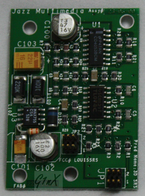
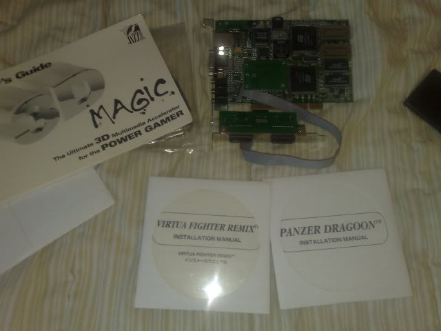
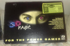
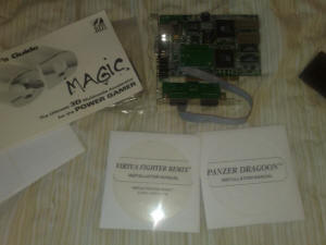
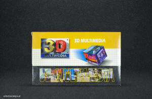
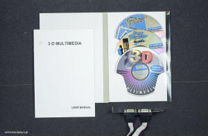
1.4 Jazz Multimedia
NOVEMBER 1, 1995 - Jazz Multimedia, Inc. announced the introduction of
3D Magic.
Jazz's 3D Magic is based on the same technology as Diamond's Edge 3D
card, but 3D Magic actually surpasses it with features not offered by
any other 3D accelerator card manufacturer, such as built-in SRS™ 3D
sound and the availability of a Jazz Output to TV Projection Card
option. Thus, all 3D game titles and software ported to nVIDIA will run
perfectly with Jazz's 3D Magic, including Sega titles.
There are two DRAM versions of 3-D Magic, based on SGS THOMSON'S STG2000
multimedia accelerator chip. The 3-D Magic 1MB DRAM version will have an
expected street price of $239.00 and a 2MB version will be priced at
around $289.00. Two VRAM configurations, based on nVIDIA Corp's NV1
multimedia accelerator chip, are also available for PCI in a 2MB
version, for approximately $339.00 -- and a 4MB version to sell for
around $489.00. Jazz Multimedia's 3D Magic in Q1 in 1996, at most major
computer retail outlets bundled with several exciting 3D game titles.
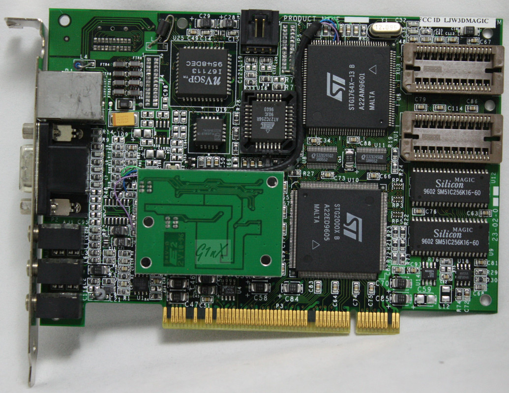
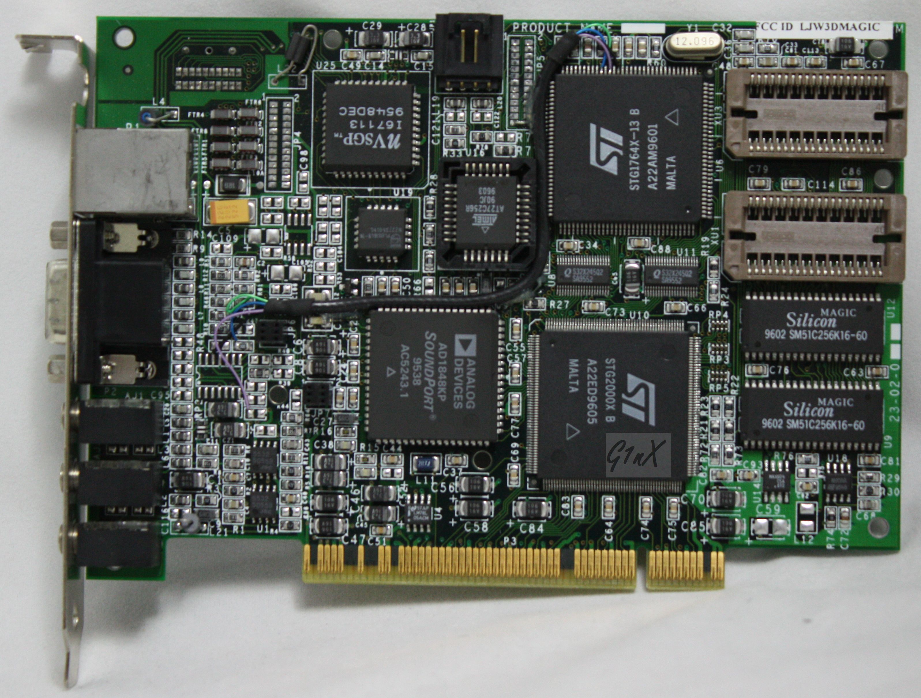
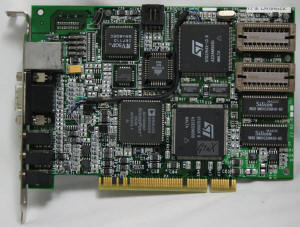
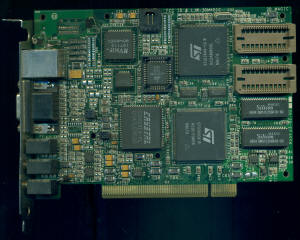
1.4.1 3D Magic DRAM(STG2000X chip)
1.4.1.1 Early Engineering sample
The early Engineering sample did not use the STG2000X of the DRAM memory
version but the all-round NV1 chip.
(From weirdo on twitter.com )
1.4.1.2 Late Engineering sample


Generally, it is possible to print the FCCID on the engineering sample
card, because you can select the code first, and then register the
selected code. There is no need to paste FCCID on engineering samples,
unless it is evaluated, displayed, and sold directly, which is very
likely. There are often engineering sample graphics cards that are
packaged for retail sale, which should be the case for this graphics
card.
1.4.1.3 Official product
(From segaretro.org)
This graphics card is Rev 2, which is more like ES than the Rev 0
graphics card above. One is that there are still many flying lines, the
other is Full PCI connection finger, and the third is to use more
tantalum capacitors. Therefore, JAZZ took out the ES with intact
performance for retail, and users could not tell.
(Fro Dav)
1.4.2 3D Magic VRAM (NV1 chip)
The VRAM version of the graphics card is more difficult to design, and
the JAZZ R&D capabilities are limited, so this version was finally
abandoned.
JAZZ was unsuccessful in NV1 and later switched to 3Dfx.
1.5 YUAN
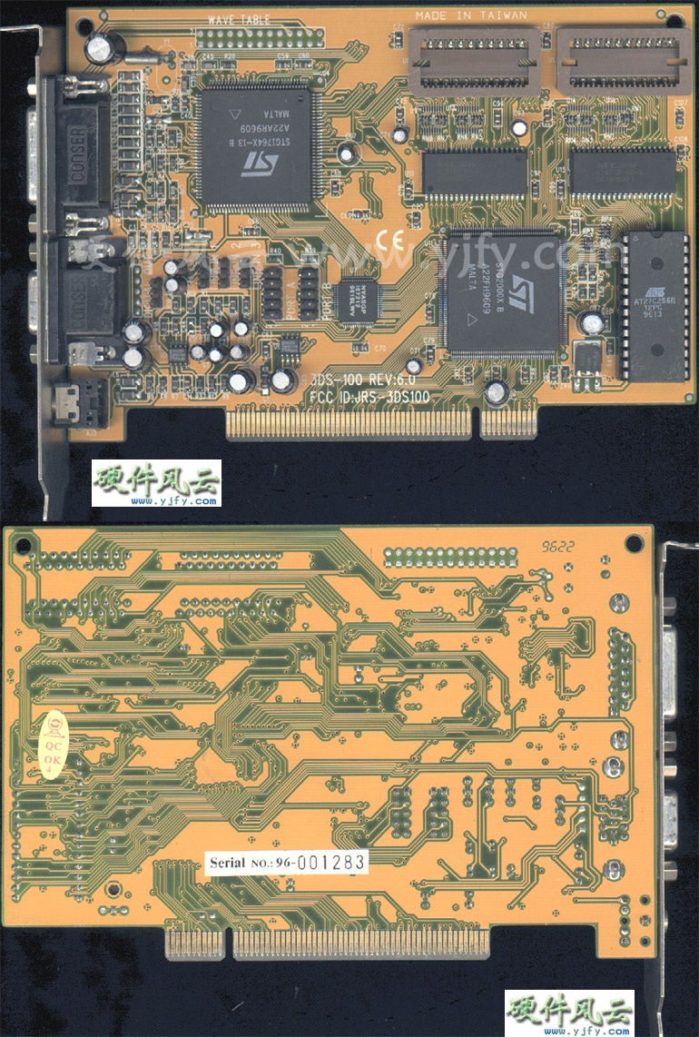
There are three revised versions of JRS-3DS100, from which we can see
the obvious changes, using a more compact package of NVSGP chip;
canceling the sound card with poor performance. Almost all manufacturers
that produce NV1/STG2000X chip graphics cards later do this.
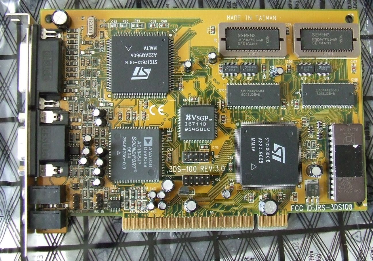
1.5.1 JRS-3DS100 V3.0
(From enacademic.com)
1.5.2 JRS-3DS100 V6.0
It was planned to be equipped with Wave table.
1.5.3 JRS-3DS100 V6.8
(From vogons.org)
|
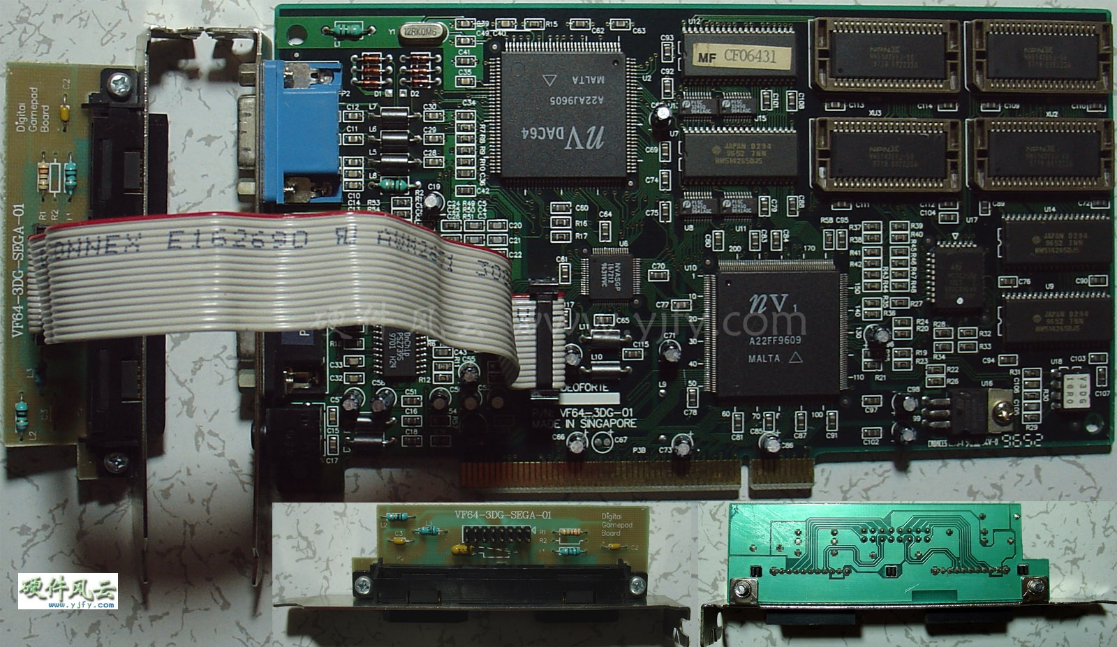
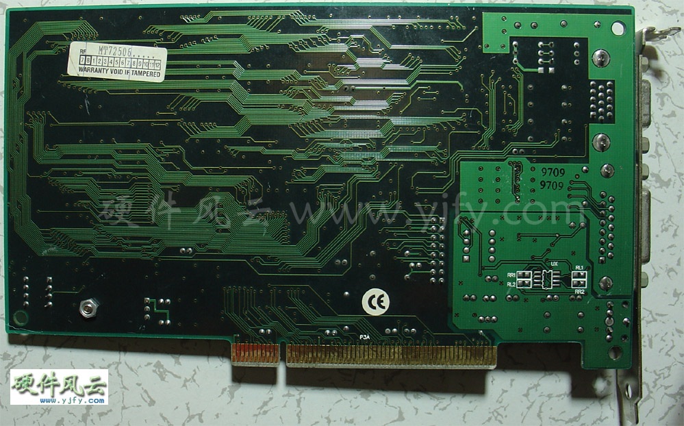
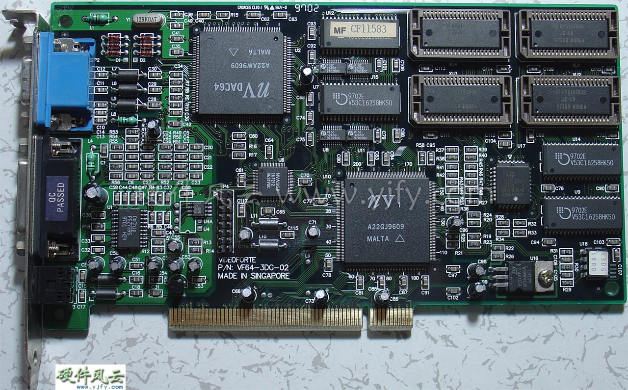
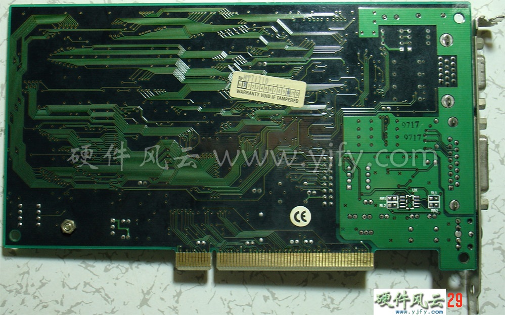
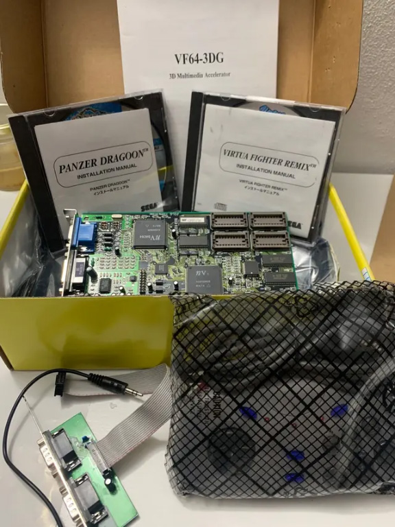
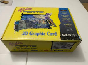
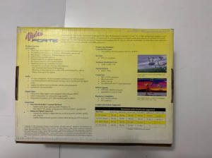
1.6 VIDEOFORTE
VIDEOFORTE's VF64-3DG graphics card appeared late, nearly 1997. It uses
NV1 chip, but instead of VRAM, it uses 2/4MB DRAM. There is no
difference between the two sub-models.
1.6.1 VF64-3DG-01
1.6.2 VF64-3DG-02
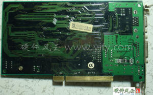
(From es.wallapop.com)

|
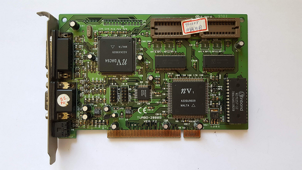
1.7 Generic
Turbo 2000B VER F2 uses NV1 chip, 1/2MB DRAM.
(From taiwan999.pixnet.net)
(FROM eBay.com)
1.8 Other
2/1/96,Genoa Introduces 3D Multimedia Accelerator Card(Stratos 3D) with
High End Graphics and SRS 3D Sound based on the NV1/STG2000.This is the
information released by nVIDIA that year, and no actual objects and
pictures have been seen. Aztech's 3D Galaxy; Kasan Electronics' WinX 3D;
Core-Dynamics' DynaGraFx 3-D and Focus TNC also launched NV1/STG2000X
chip graphics cards, none of which have seen the actual objects and
pictures. |
NV2
July 31, 1995 Sega of America, Inc., is setting a new standard in
gameplay for personal computers through an exclusive licensing agreement
with nVIDIA;
Sega's high-end Sega Saturn and arcade software to CD-ROMs for
Pentium-based PCs equipped with single-chip NV1 Multimedia Accelerator.
Sega PC CD-ROM games developed for the nVIDIA architecture deliver the
next level of multimedia entertainment under Windows 95 and have the
same stunning visuals and gameplay of the Sega Saturn versions.
January 9, 1996 Sega PC's Panzer Dragoon to be bundled with Diamond EDGE
3D Multimedia Accelerators for Personal Computers
Thanks to Sega's strong support, nVIDIA's NV1 chip finally got some
applications. But nVIDIA is still in a difficult situation.
Due to nVIDIA's strong desire to stick with their maturing quadratic
forward texture mapping technology, but polygon rendering was the way to
go for the future.Sega and nVIDIA have conflicts.
Sega ultimately selected NEC/VideoLogic's PowerVR2 to power the
3d-graphics in its Dreamcast console.NV2 was finally cancelled. |
3. NV3
3.1 nVIDIA
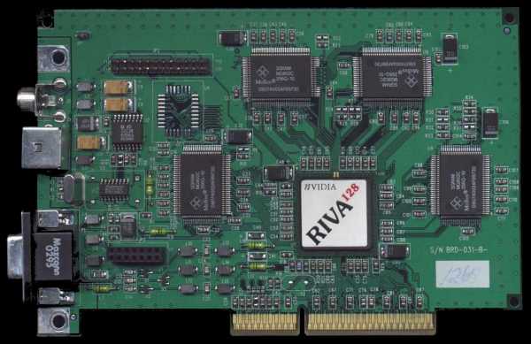
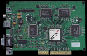
3.1.1 Riva 128
April 8, 1997- SGS-THOMSON Microelectronics, Inc. and nVIDIATM
Corporation jointly introduced RIVA 128, the first 128-bit 3D multimedia
accelerator.
August 25, 1997- nVIDIA Corporation announced its RIVA 128 3D multimedia
accelerator has been selected by five major OEMs including Dell
Computer, Gateway 2000, Micron Electronics, and graphics accelerator
manufacturers Diamond Multimedia Systems Inc. and STB Systems Inc.
0.35 micron
3.5 million transistors
5M triangles/sec, 100M pixels/sec
3.5 million transistors
12 KB on chip memory
20 billion operations per second
128-bit pipeline and memory interface
100 MHz CLK speed
128-bit engine, 128-bit memory interface
100 MHz sgram interface - 1.6 gbytes/sec bandwidth
206 MHz integrated ramdac
NTSC/PAL output
With the popularity of Windows95, nVIDIA will not make mistakes like NV1
and NV2 again this time. Since the strength is not enough to make rules,
then follow the trend. NV3 regards Microsoft's Direct3D as the priority
API, which is very correct and lays a solid foundation for future
development.
3.1.1 nVIDIA
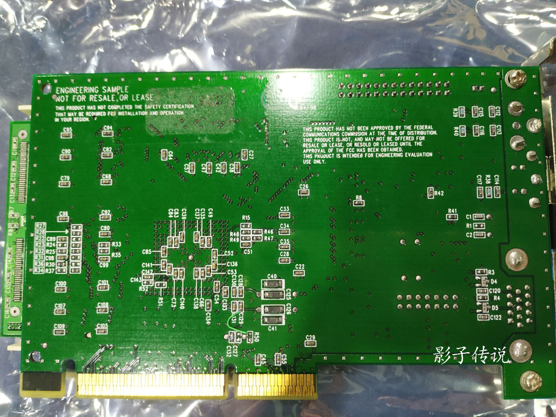
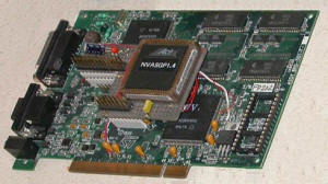
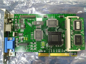
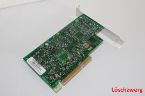
3.1.1.1 Riva 128 Engineering sample
This is the Product Evaluation board, which is also a reference board.
Many graphics cards look close to this.
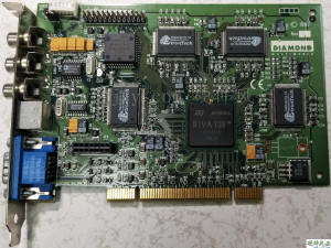
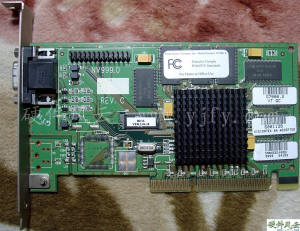
3.1.2 Riva 128ZX
February 23, 1998 nVIDIA Corporation unveiled the RIVA 128ZX processor.
Coupled with new enhanced ZX software drivers, the RIVA 128ZX processor
offers the industry's fastest 3D processing capability , extended
resolution and color depth, AGP 2X support, as well as high-performance
2D, VGA and digital video capabilities.
The PCB date of this Product Evaluation board is 9804 weeks, and the
release date is 9809 weeks.

This is the earliest sample of nVIDIA's graphics card in the hands of
known collectors.
|
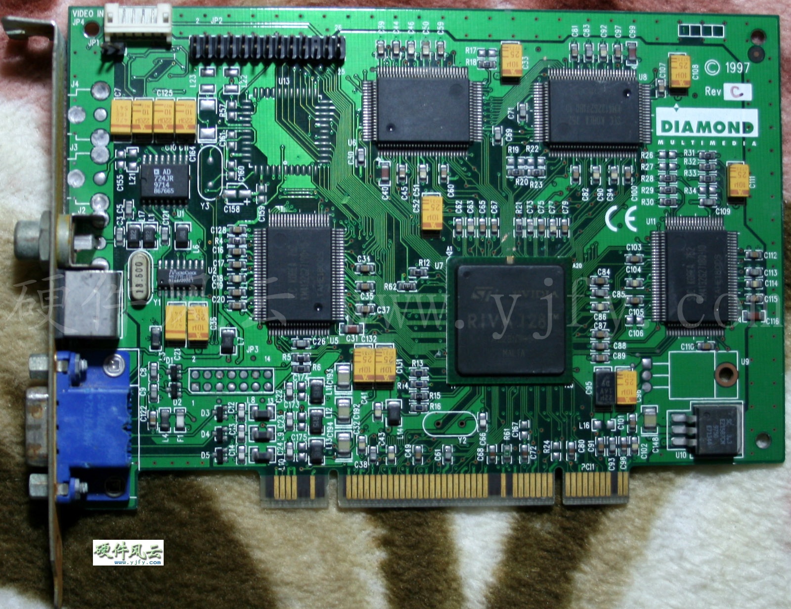
3.2 Diamond
Diamond was unsuccessful in the NV1 graphics card project, which caused
Diamond to lose confidence in nVIDIA and instead supported another new
company, 3DFX. As a result, STB took the lead in the NV3 graphics card
project.
Although Diamond is half-hearted on the NV3 graphics card, it has
launched four board-type Viper V330 graphics cards, which are of decent
design and workmanship and have achieved certain success.
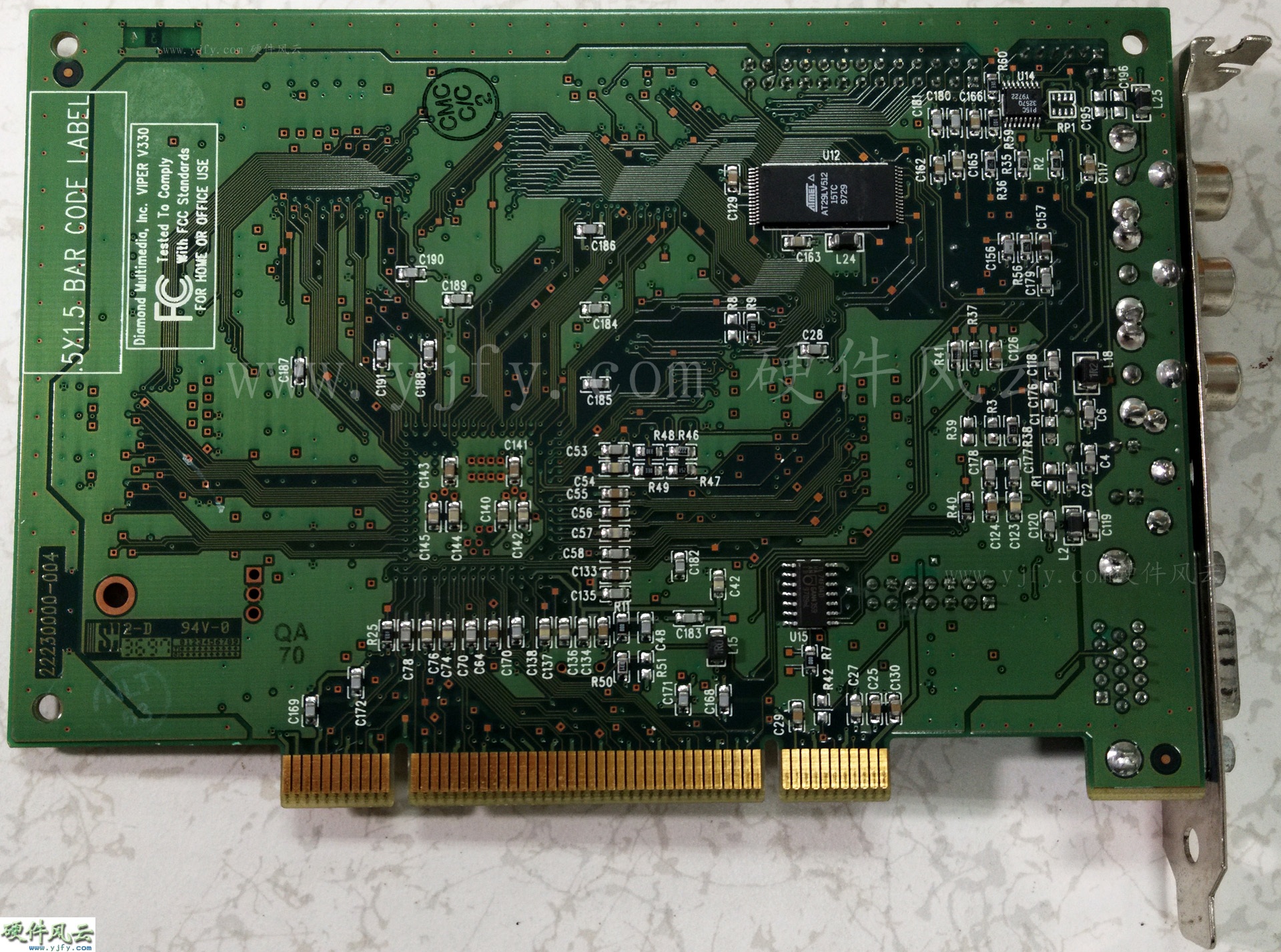
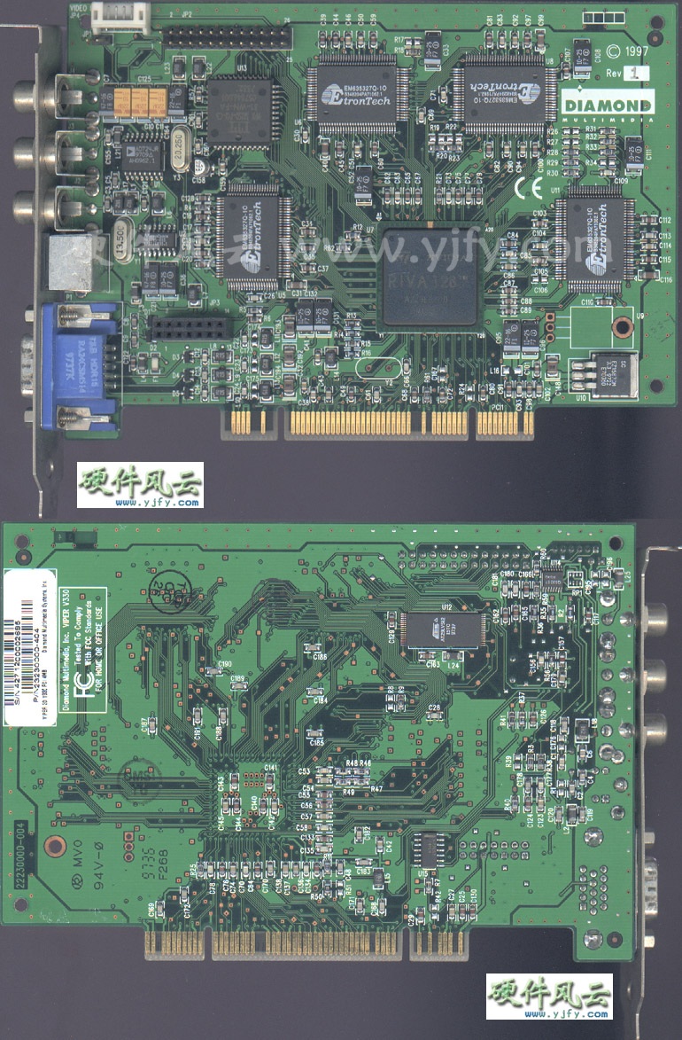
3.2.1 Viper V330 VIVO AGP/PCI
3.2.1.1 ES
On August 25, 1997 (9735 week), nVIDIA announced that Diamond and STB
had joined the ranks of riva128 graphics cards. At that time, the
research and development of STB's VELOCITY 128 graphics card was
completed, and it will be used on branded machines in September. What is
the progress of Diamond's Viper V330 graphics card? Take a look at the
Viper V330 engineering sample graphics card below and maybe give the
answer.

The PCB date of the above card is 9736 weeks, which is more than one
week later than nVIDIA's announcement date. After all, testing also
takes time. The PCB date of the earliest official version of the Viper
V330 graphics card is also 9736 weeks, and the 9736 week finalization
date has been approved.
The Riva 128 chip date of this engineering sample graphics card is 9731
weeks, which is pretty early, and the graphics card is made in the
United States. It can be seen that the positions and quantities of many
resistors and capacitors are slightly different from the official
version. If you are interested, you can compare them; the ITT video chip
is also an ES version;full
gold finger. Based on the consideration of manufacturing cost,
Diamond first conducted small-batch R&D in the United States and
mass-produced in Taiwan.
Viper V330 graphics cards began to advertise in November, and retail
time is around October.
I spent $1,000 on this Viper V330 engineering sample graphics card.If
you want to collect rare collectibles, if you don't have the luck to buy
cheap ones, you have to be willing to spend money.
Most of the engineering samples are kept in small quantities, and many
of them are orphans. If they are missed, they will never be met again.
3.2.1.2 QS
(From thg.ru)
This kind of graphics card has been distributed to evaluation agencies,
but no retail.
3.2.1.3 Official product
3.2.1.3.1 VIVO
The full version of the VIVO version is very exquisite, and the number
is very small. Few people can collect it.
|
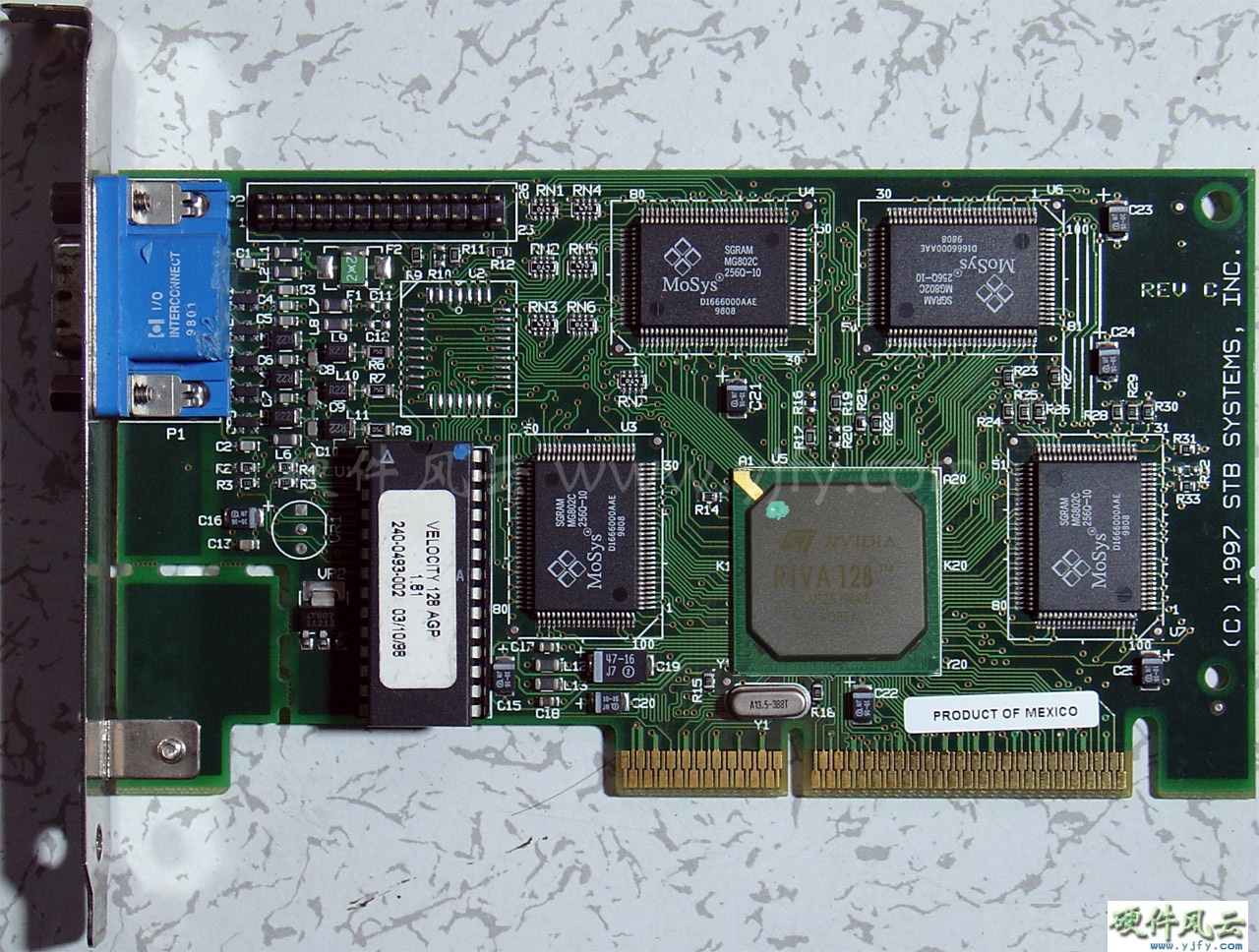
3.3 STB
STB believes that future growth was dependant upon the successful
introduction of a new generation of multimedia accelerators.STB is the
first to cooperate with nVIDIA, obtain the latest RIVA 128 graphics
engine produced, and develop Velocity 128 graphics card.
In June 1997, STB began extensive testing of the Velocity 128. STB
results of performance tests conducted on the Velocity 128 which proved
that the nVIDIA RIVA128 graphics engine was defective and was causing
PC's in which it was installed to crash.
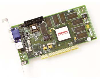
VELOCITY 128
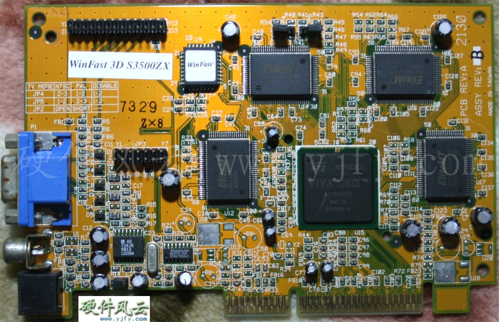
3.4 Leadtek
S3500ZX

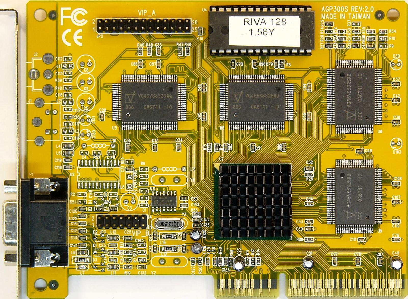
3.5 YUAN
AGP300S
(From Palcal on vgamuseum.info)
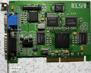
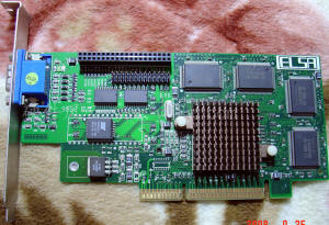
3.6 ELSA
Victory Erazor
3.7 ASUS
3DP-V3000
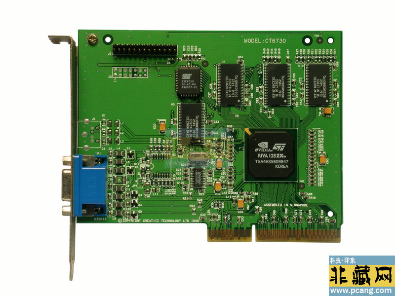
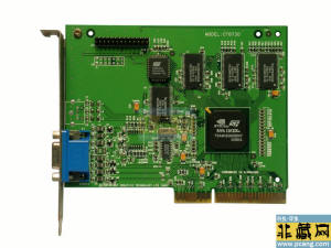
3.8 Creative
CT6730
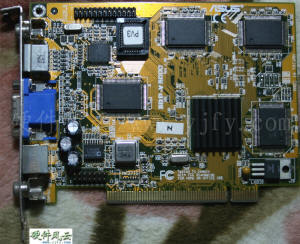
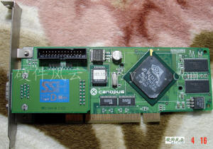
3.9 Canopus
TOTAL3D 128
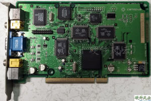
This board is the largest.
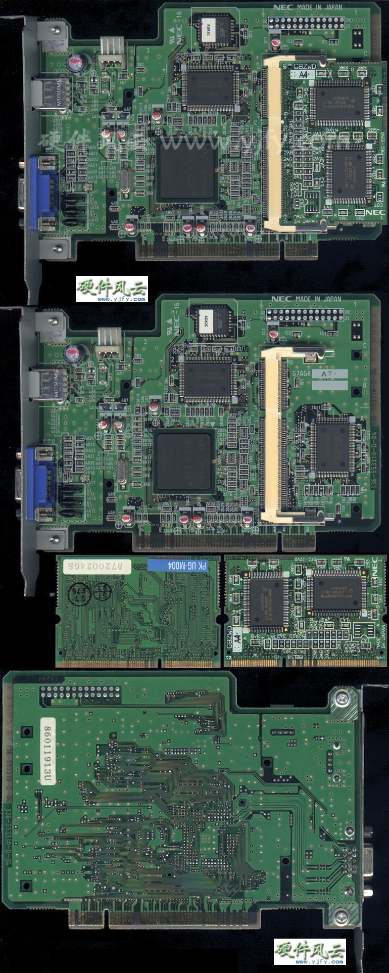
3.10 NEC
G7AGK
The use of extended video memory design is rare.
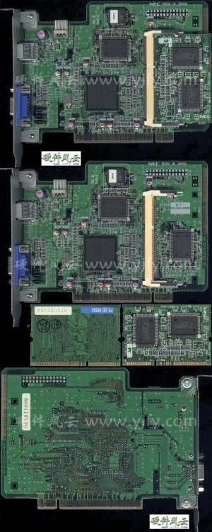
3.11 I-O DATA
GA-ZXTV8/PCI-1
nVIDIA RIVA 128ZX
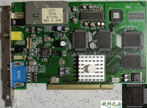
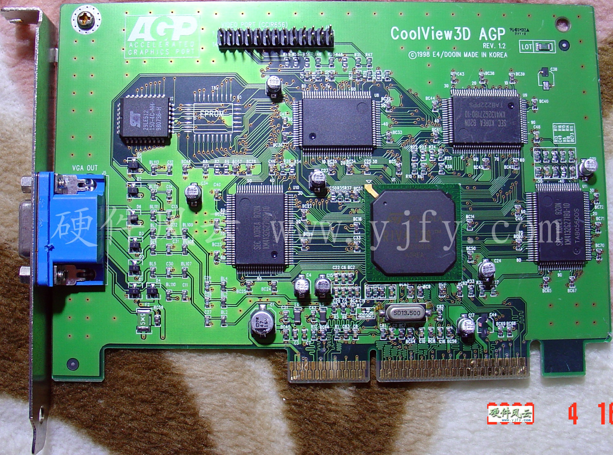
3.12 E4/DOOIN
CoolView3D AGP
This card can support dual EPROM, but I don't know what it is for.
 |
4. NV4
July 31, 1998nVIDIA's RIVA TNT 3D PROCESSOR
Riva TNT defeated the incredible 3Dfx Voodoo 2 and became the
fastest graphics card of the year, and nVIDIA also noticed the
importance of excellent drivers to give full play to the performance
of the graphics chip, and wrote a new driver for RIVA TNT and named
it As "Detonator"
TNT is the abbreviation of Twin Texel. The core architecture is a
rendering system with two 32-bit pixel pipelines, each pixel
pipeline has 1 TMU, and two textures are processed in parallel in
each clock cycle. In this way, the maximum fill rate of RivaTNT
working at 90MHz can reach 180M Texels/sec. At the same time, Riva
TNT also has a 24-bit Z buffer (Z-Buffer) and an 8-bit stencil
buffer for the first time.
TNT's design goal was to achieve twice the performance of Voodoo2,
but because the 0.25 micron process was not perfect at the time,
nVIDIA had to use a 0.35 micron process, making RivaTNT only work at
90MHz.
4.1 nVIDIA
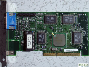
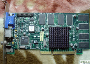
4.1.1 Chip Evaluation board

(From anandtech.com)
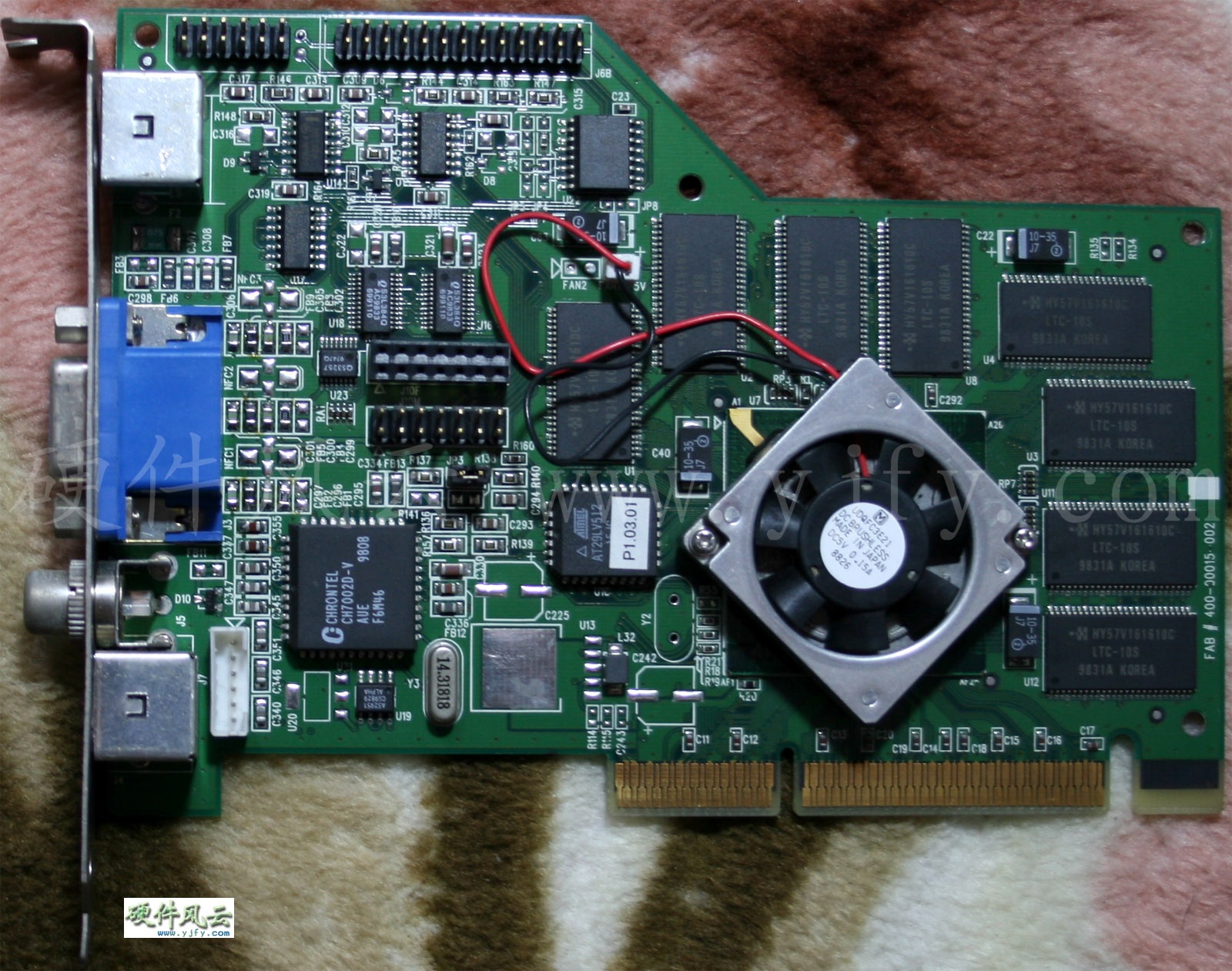
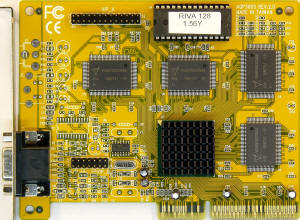
4.1.2 Product Evaluation board
nVIDIA's Product Evaluation board is the later public version or
reference board, and many manufacturers' graphics cards use this
layout more or less.
(From PC Mag December 1, 1998)
|
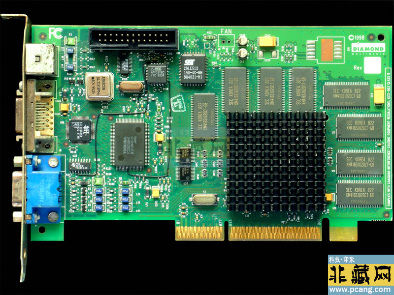
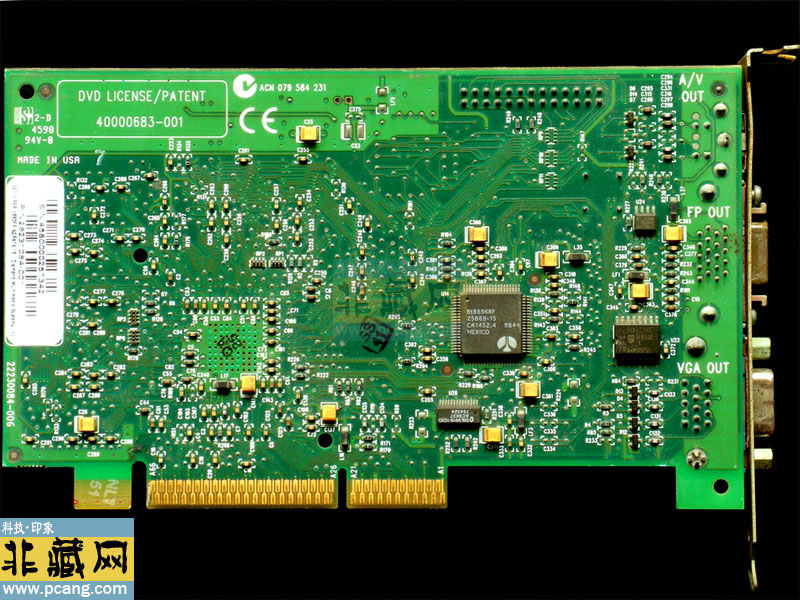
4.2 Diamond
The NV3 graphics card project finally succeeded, and the Voodoo card
supported by Diamond was also successful. Diamond was unable to tilt
the NV4 graphics card project. There are only four types of Viper
V550 graphics cards.
4.2.1 Viper V550 VIVO AGP/PCI
Although the two versions of Viper V550 graphics cards are VIVO
versions, in fact very few have VIVO, most of them are TV-OUT Viper
V550 graphics cards.
4.2.1.1 ES
This is the official promotional image of Diamond, which was later
printed on the box.
(From assets.hardwarezone.com)
4.2.1.2 PCI
The most common is the TV-out version, but I haven't seen the VIVO
version.
4.2.1.3 AGP
The most common is the TV-out version, and the VIVO version is very
rare.

(From Amibay.com)
4.2.2 Viper V550 NLX AGP
4.2.2.1 QS
This is the official promotional image of Diamond, which was later
printed on the box. Like the official product, it is QS.

(From home.datacomm.ch)
4.2.2.2 Official product
4.2.3
Viper V550 FP AGP
This model is an OEM version.
4.2.3.1
ES
After disassembling the machine, Diamond sends fully functional
engineering samples to the manufacturer for use.
4.2.3.2 Official product
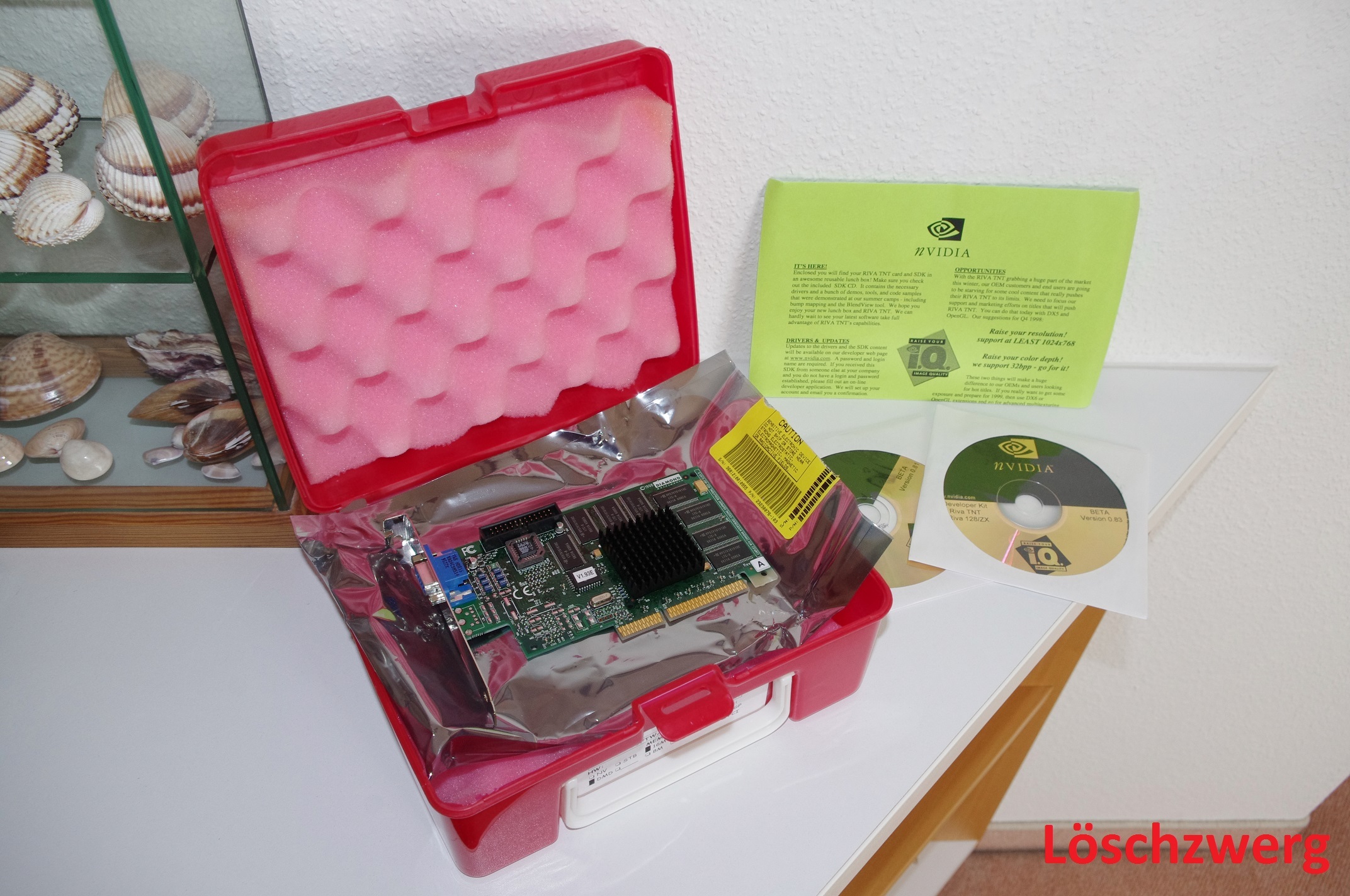
4.2.4 Riva TNT SDK
nVIDIA and STB graphics cards are optional for this component. I
have an empty box to select STB.
nVIDIA also presents engineering sample graphics cards in gift boxes
to important customers.
4.3 STB
Velocity 4400
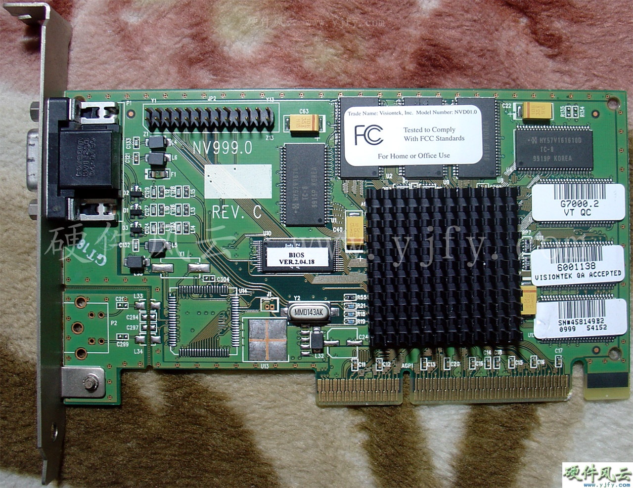
4.4 Visiontek
NVD01.0, this board type is very close to nVIDIA's Product
Evaluation board.
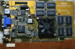
4.5 ASUS
AGP-V3400TNT
4.6 Canopus
SPECTRA 5400

4.7.ELSA
VICTORY II-A16
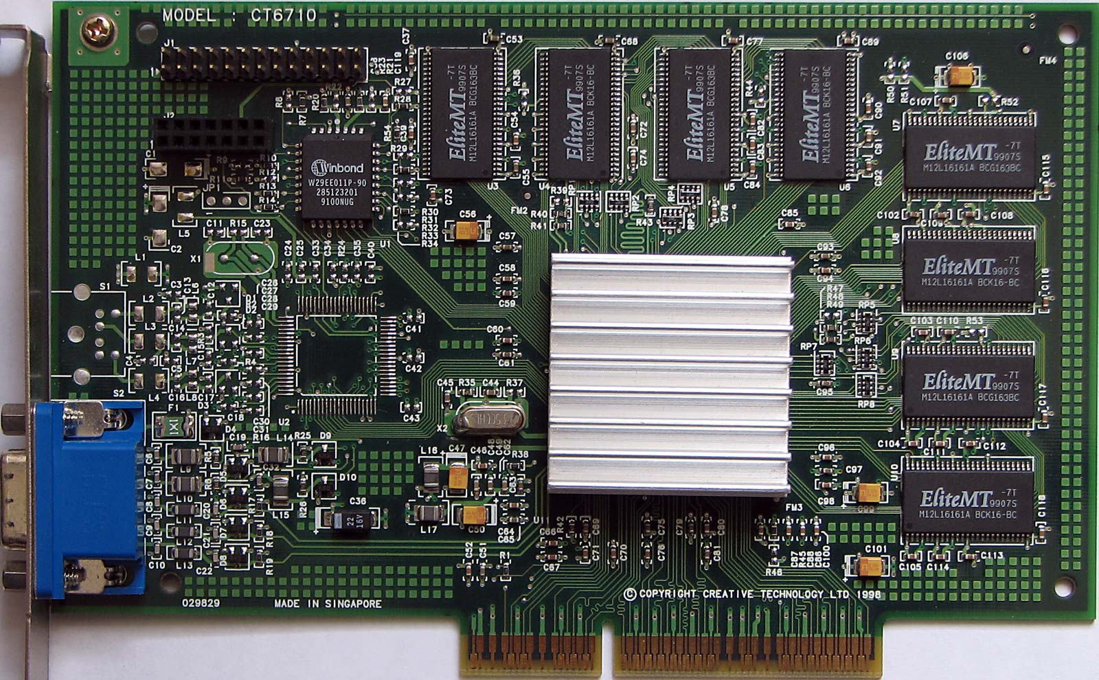
4.8 Creative
CT6710
(From Vlask on vgamuseum.info)
4.9 Hercules
Dynamite TNT
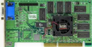
(From Palcal on vgamuseum.info) |
5. NV5 & NV6
Release Date:Mar 15th, 1999
The nVIDIA TNT2 was the first chipset to offer a 32-bit frame buffer
for better quality visuals at higher resolutions, 32-bit color for
more realistic colors, and a 32-bit Z/stencil buffer for incredible
3D effects―blazing
The TNT2 family is the first product line to offer "top-to-bottom"
chips to satisfy the needs of every computer and user in the
spectrum from basic to high-performance desktop PC computing.
The core code of Riva TNT2 is NV5, which is the cornerstone of
nVIDIA's graphics dynasty so far. Thanks to the 0.25 micron process,
the frequency of the nVIDIA Riva TNT2 Standard Edition has been
increased to 125MHz. The frequency increase and the optimization of
the core internals, the performance of nVIDIA Riva TNT2 With a big
leap, the performance was unmatched at the time. In the later
period, nVIDIA Riva TNT2 also uses NV6 with a 0.22 micron process,
and the frequency is further improved.
Beginning with nVIDIA Riva TNT2, nVIDIA has marketed its products.
At the high, middle and low end, nVIDIA Riva TNT2 chip derives TNT2
Ultra, TNT2 Pro, TNT2 M64, TNT2 Vanta, TNT2 Vanta LT, etc. Different
models of products, with different capacities of video memory, the
product line covers most of the market.
TNT2
Memory Speed:150 MHz
Pixels Per Second:230 Million
Memory Bandwidth:2.4GB/s
TNT2 Ultra
Memory Speed:183 MHz
Pixels Per Second:300 Million
Memory Bandwidth:2.9GB/s
Later, with the progress of the process, NV6 also used 0.22 micron
process, Release Date Oct 12th, 1999, and was named TNT2 PRO, which
was also used in some TNT2 Ultra. After using the 0.22 micron
process, the power consumption and heat generation of TNT2 PRO have
been significantly reduced, the overclocking capability is stronger,
and the cost performance is further improved. In addition to the
high- and mid-end TNT2 standard version, nVIDIA also uses the 0.22
micron process NV6 chip to launch TNT2 Vanta and TNT2 M64 for
low-end users.
The combination of reliability, compatibility, performance, and
quality―at a low cost―has made nVIDIA Vanta the product of choice
for leading OEMs and system integrators. The nVIDIA Vanta comes in
4-16MB configurations.
TNT2 Pro
Memory Speed:166 MHz
Pixels Per Second:284 Million
Memory Bandwidth:2.65GB/s
TNT2 M64
Memory Speed: 150 MHz
Pixels Per Second:230 Million
Memory Bandwidth:1.2GB/s
Vanta
Graphics Core:128-bit
Pixels per Second:200 Million
Memory Bandwidth:1.0GB/s
Vanta LT
Graphics Core:128-bit
Pixels per Second:160 Million
Memory Bandwidth:800 MB/s
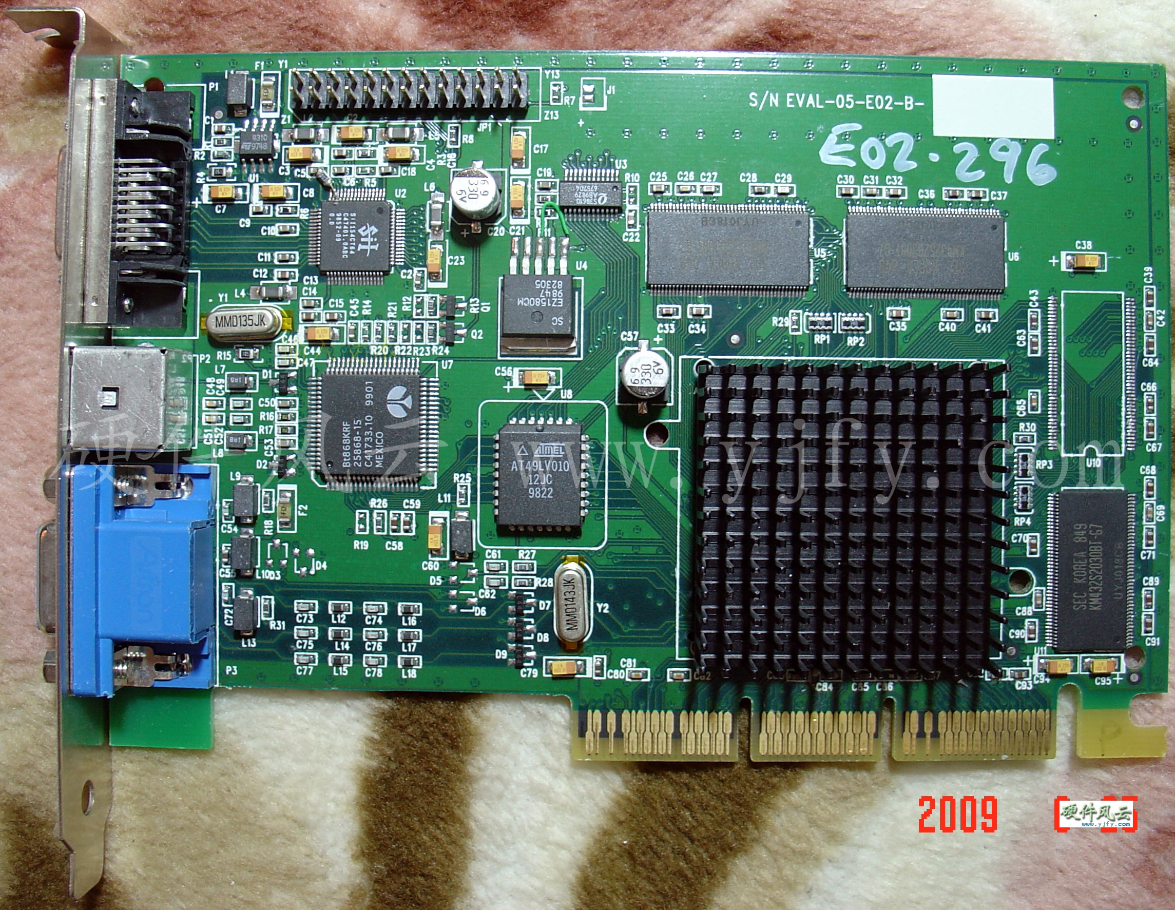
5.1 nVIDIA
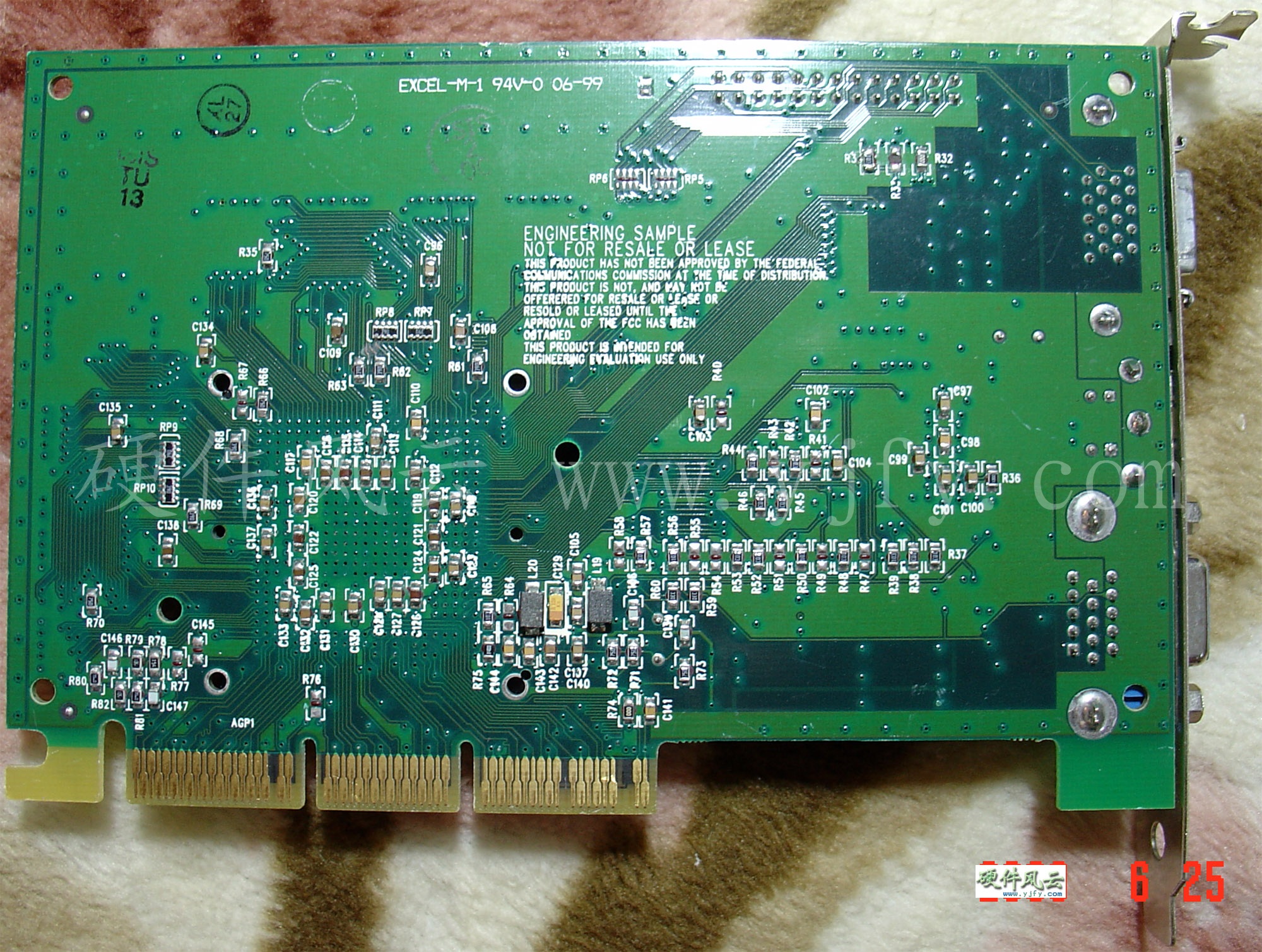
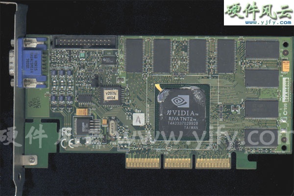
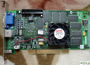
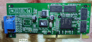
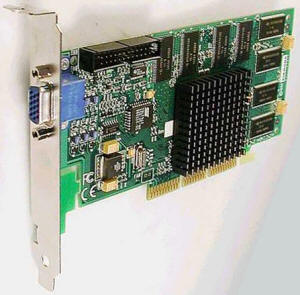
5.1.1 ES
5.1.1.1 CHIP EVALUATION board
The PCB date of the graphics card is 9850 weeks, earlier than the
release date of Mar 15th, 1999 (9915 weeks).
TNT2 CHIP EVALUATION board
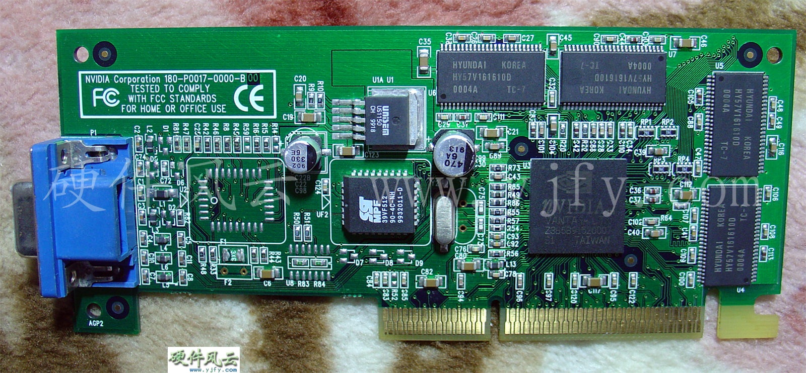
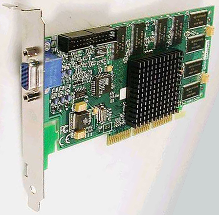
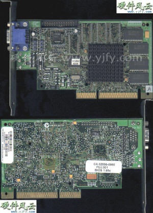
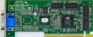
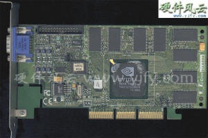
5.1.1.2 PRODUCT EVALUATION board
PCB date 9906 weeks, earlier than the release date Mar 15th, 1999
(9915 weeks).
TNT2 PRODUCT EVALUATION board

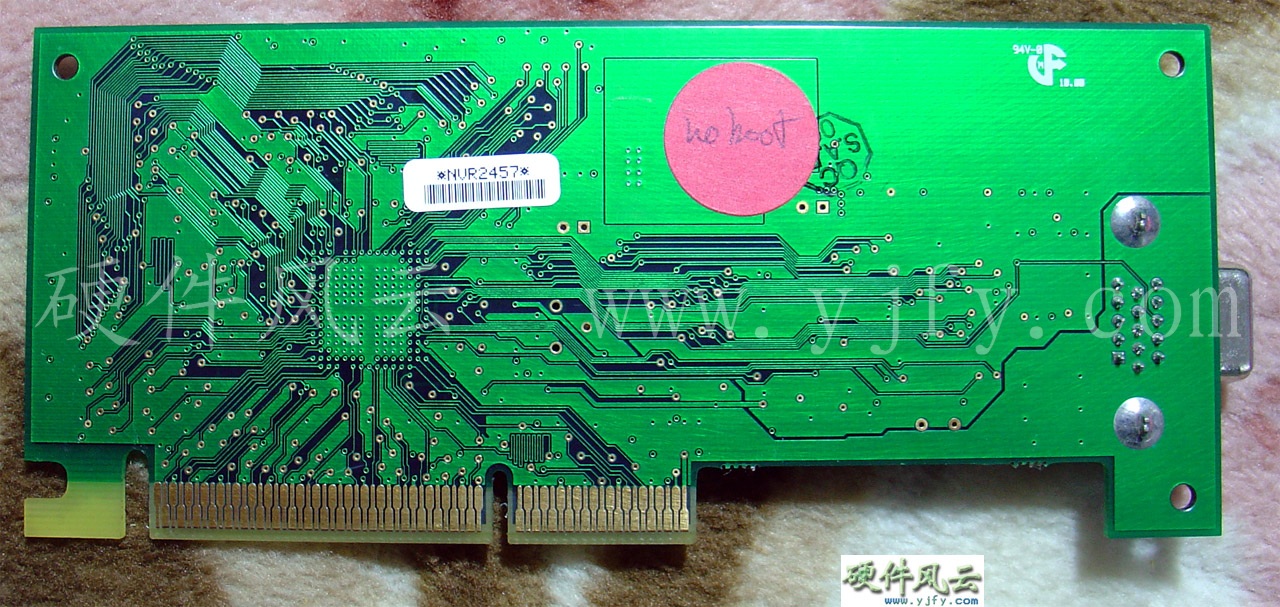
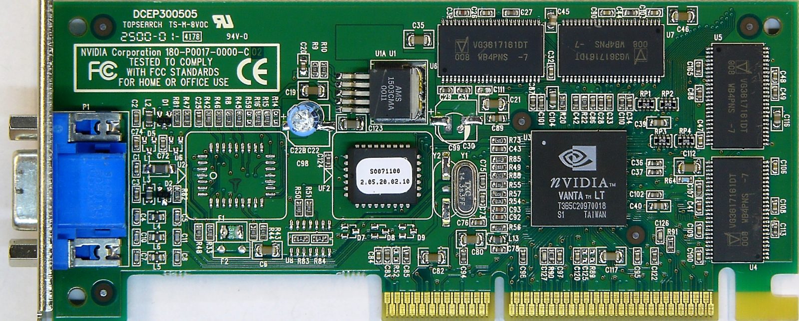
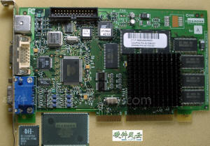
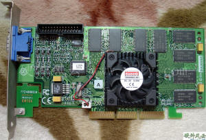
5.1.1.3 Reference board
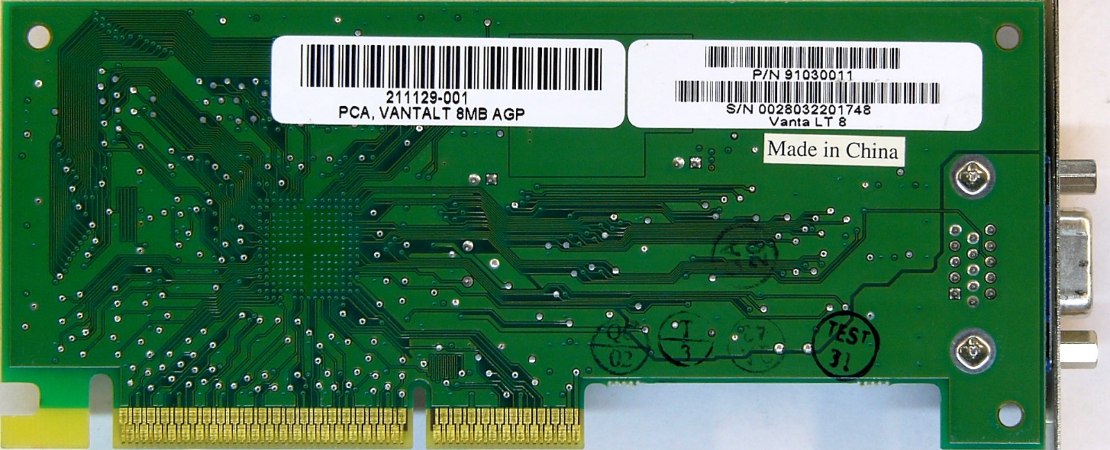
PCB date is 0010 week, and the release date is March 1, 2000 (0010
week).
VANTA LT Reference board
The above graphics card is the public version or reference board
often referred to now. The following graphics card is the
manufacturer's public graphics card.
(From Palcal on vgamuseum.info) |
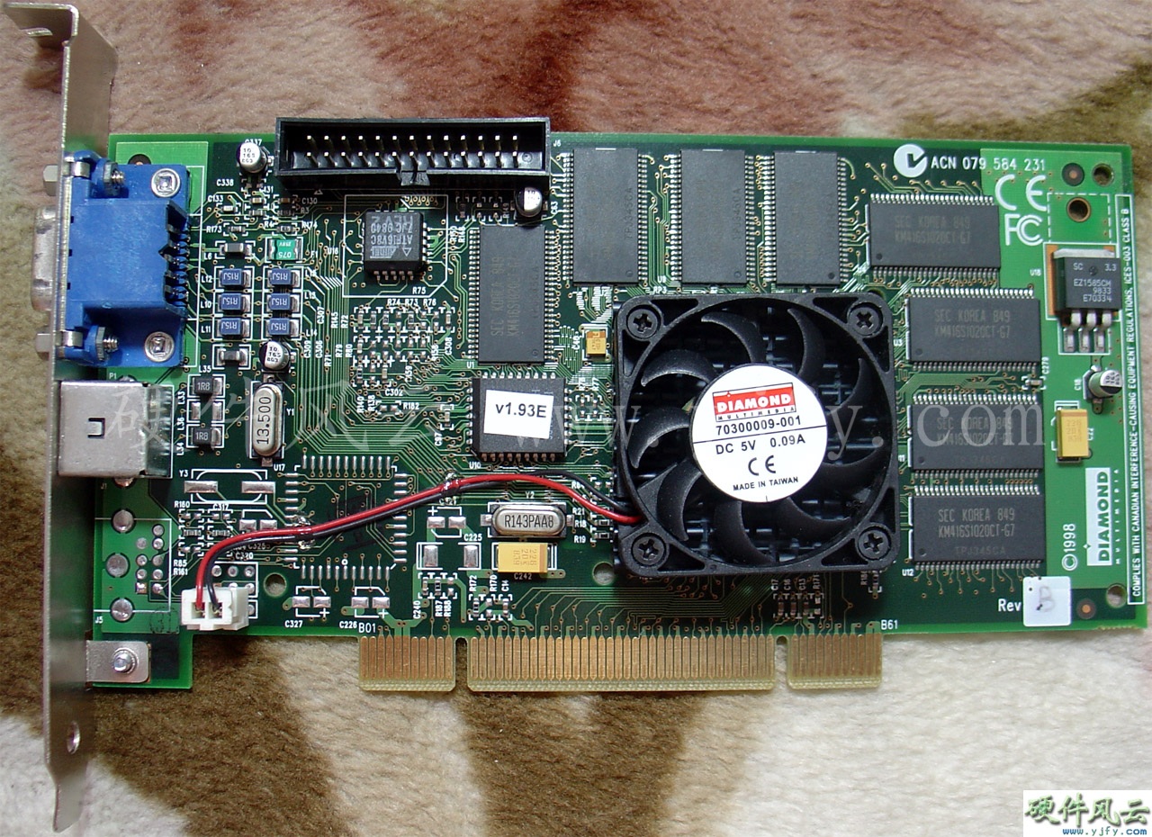
5.2 Diamond
5.2.1 VIPER V770 ES
(From home.datacomm.ch)
5.2.2 VIPER V770
TNT2 chip
5.2.2 VIPER V770 Ultra
TNT2 Ultra chip
5.2.2 VIPER V730
Vanta chip
The PCB date of this graphics card is 9923 weeks, and Diamond
was acquired by S3 on June 22, 1999 (9926 week).
It is a PCB board made before the acquisition. The memory chip
date on the card is 9929 weeks, indicating that the card was
finally manufactured by S3.
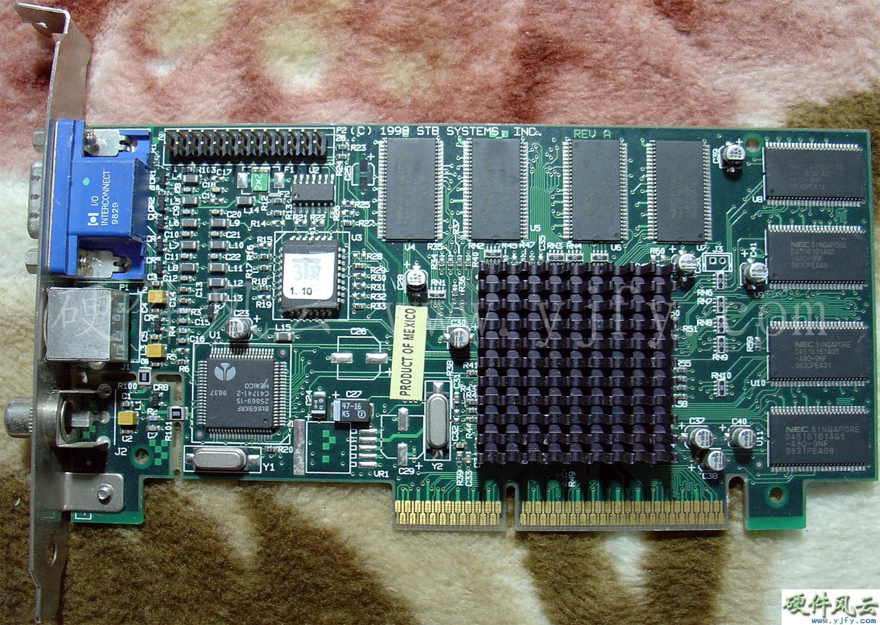
5.3 Gigabyte
5.3.1 GA-660 ES
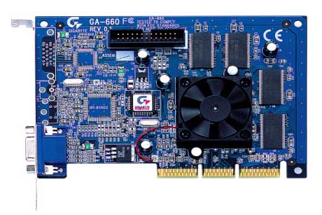
(From orlova.rsue.ru.)
5.3.2 GA-622 ES
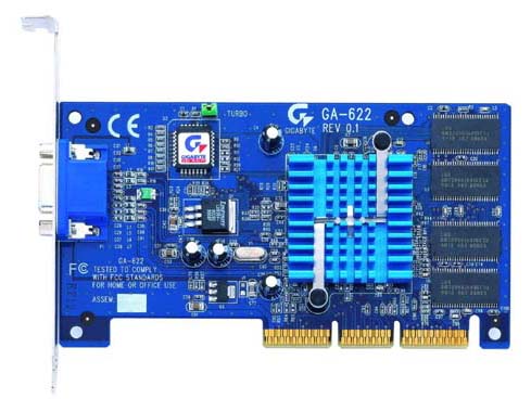
(From anandtech.com)
5.4 Creative
CT5823
5.5 ELSA
Synergy II-16
5.6 Canopus
SPECTRA Light T32PCI
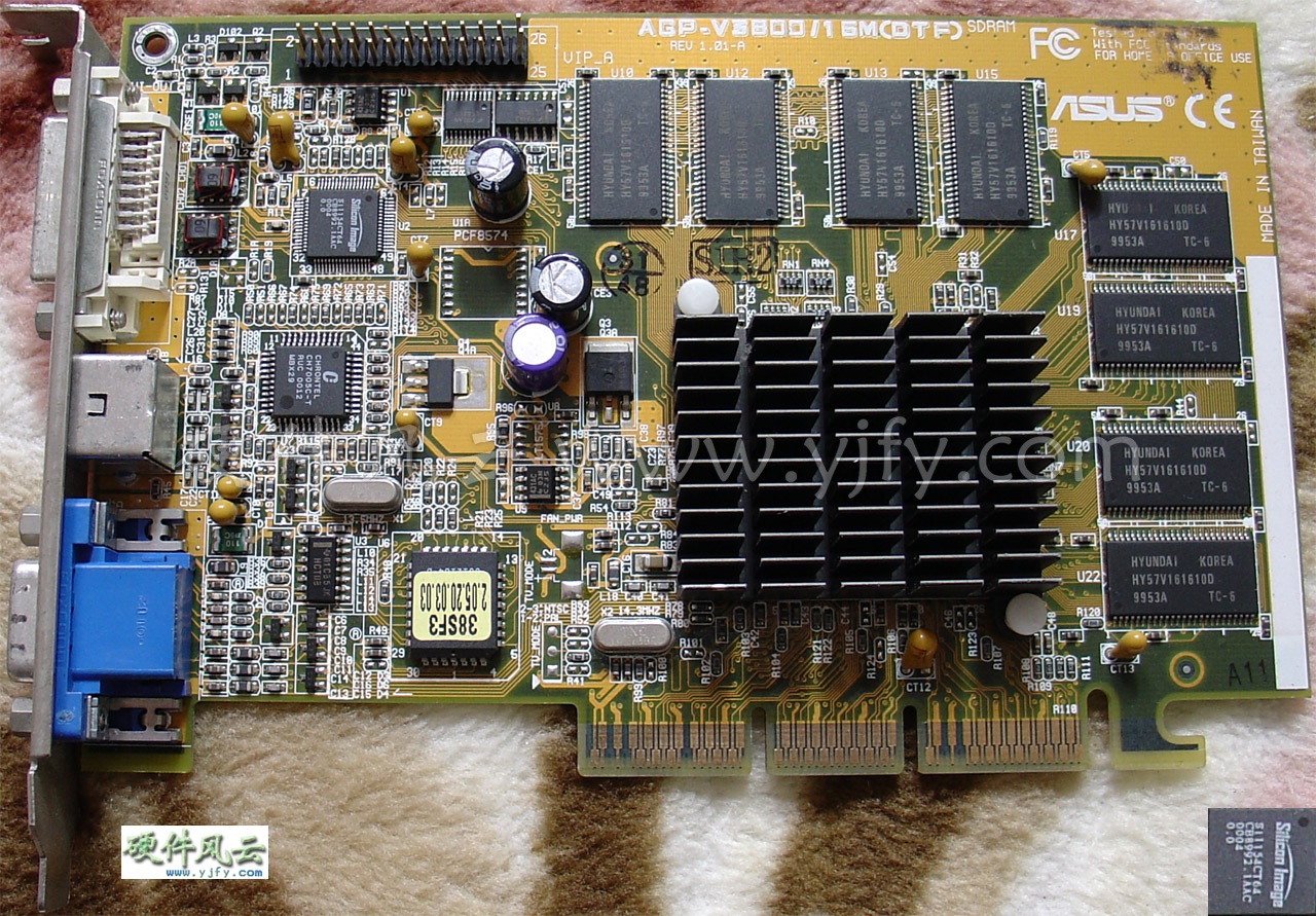
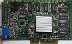
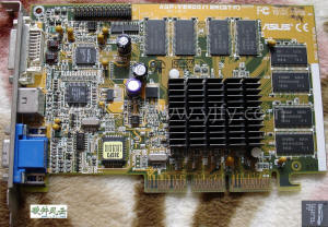
5.7 ASUS
AGP-V3800/16M(DTF)
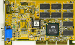
5.8 MSI
MS8807
 (From Palcal on vgamuseum.info)
It can be seen from the previous graphics cards that all
manufacturers have not completely copied the original nVIDIA
design, at most they only partially borrowed from the original
nVIDIA design. Even the public version launched by nVIDIA is not
directly used by manufacturers. In addition to the fact that
each manufacturer deliberately retains its own unique design
concepts and styles, the design and use cycle of graphics cards
is long, and everyone still has time to spend on design. But
this time that can be consumed is gradually shortening. Big
factories like STB and Dimeng were acquired in the TNT era.
After entering the GPU era, graphics cards are updated faster,
and manufacturers have to accept nVIDIA's public version design.
Graphics cards that do not use the public version design are
almost all shrunk designs and become synonymous with low-end
graphics cards. So far, almost all the graphics cards look
exactly the same, the only difference is the fan and heat sink.
Therefore, the history of nVIDIA graphics cards introduced in
the following chapters will be based on nVIDIA’s evaluation
boards and reference versions.
(From Palcal on vgamuseum.info)
It can be seen from the previous graphics cards that all
manufacturers have not completely copied the original nVIDIA
design, at most they only partially borrowed from the original
nVIDIA design. Even the public version launched by nVIDIA is not
directly used by manufacturers. In addition to the fact that
each manufacturer deliberately retains its own unique design
concepts and styles, the design and use cycle of graphics cards
is long, and everyone still has time to spend on design. But
this time that can be consumed is gradually shortening. Big
factories like STB and Dimeng were acquired in the TNT era.
After entering the GPU era, graphics cards are updated faster,
and manufacturers have to accept nVIDIA's public version design.
Graphics cards that do not use the public version design are
almost all shrunk designs and become synonymous with low-end
graphics cards. So far, almost all the graphics cards look
exactly the same, the only difference is the fan and heat sink.
Therefore, the history of nVIDIA graphics cards introduced in
the following chapters will be based on nVIDIA’s evaluation
boards and reference versions.
|
|