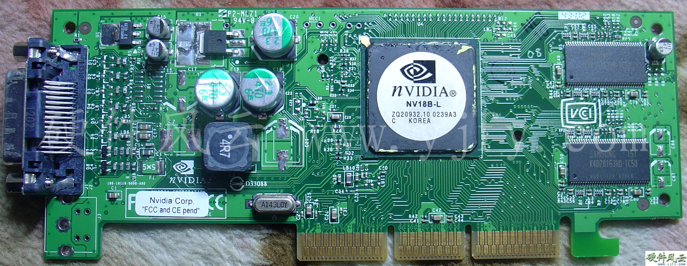
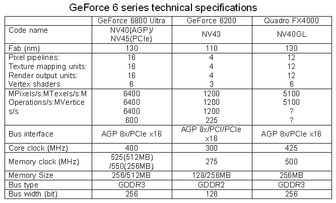
|
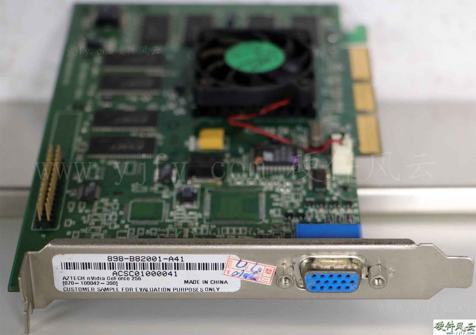
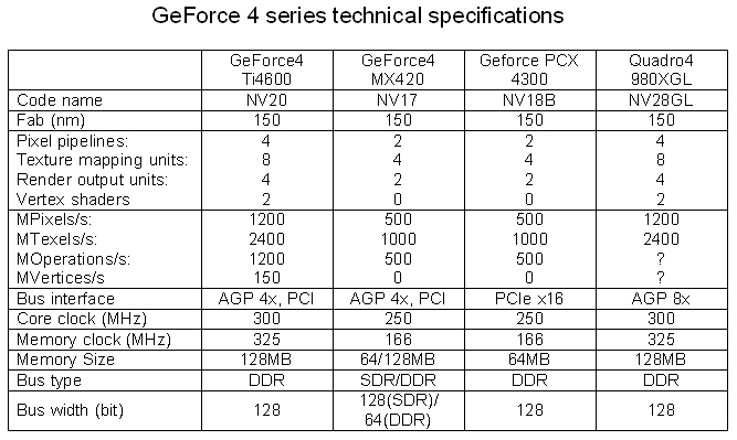
5. GeForce FX��NV30��ϵ��
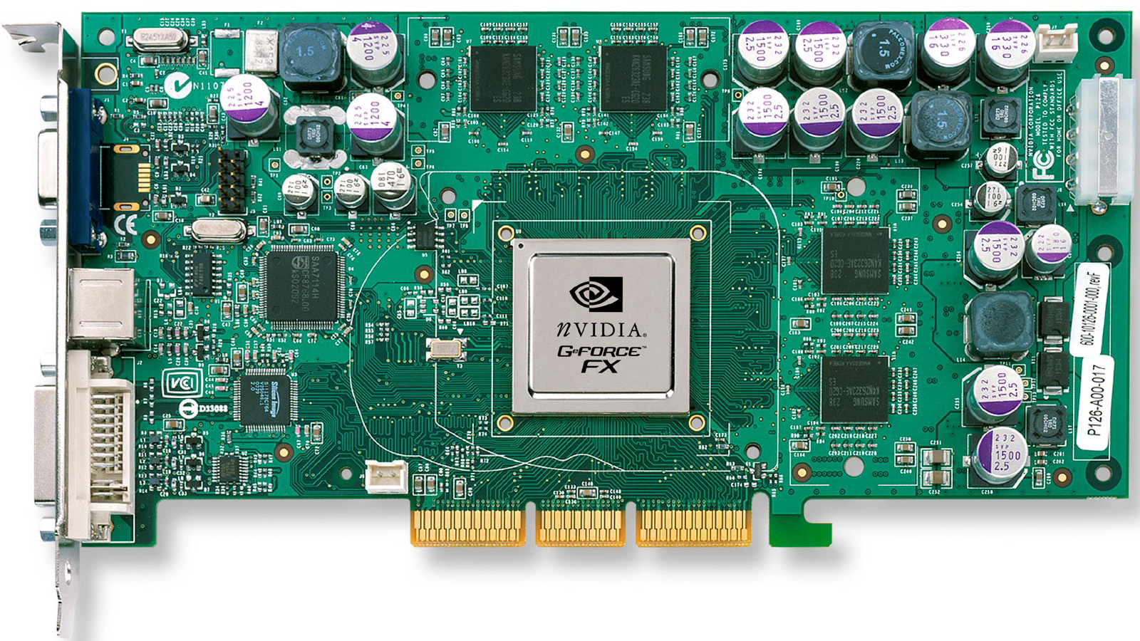
����һ����Ʊ��nVIDIA����2002��11��18�շ���GeForce FX5800/5800
Ultra�Կ���ʵ�ʷ������ڵ�������3�·ݡ�NV30оƬʹ��130
nm���������������Ƶ����400��500 MHz֮�䣬���ҿ���ͨ����800 MHz��1000 MHz���е�128λ���߷���128MB
GDDR2��
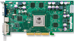
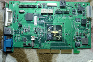
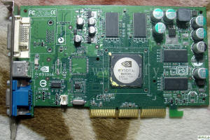
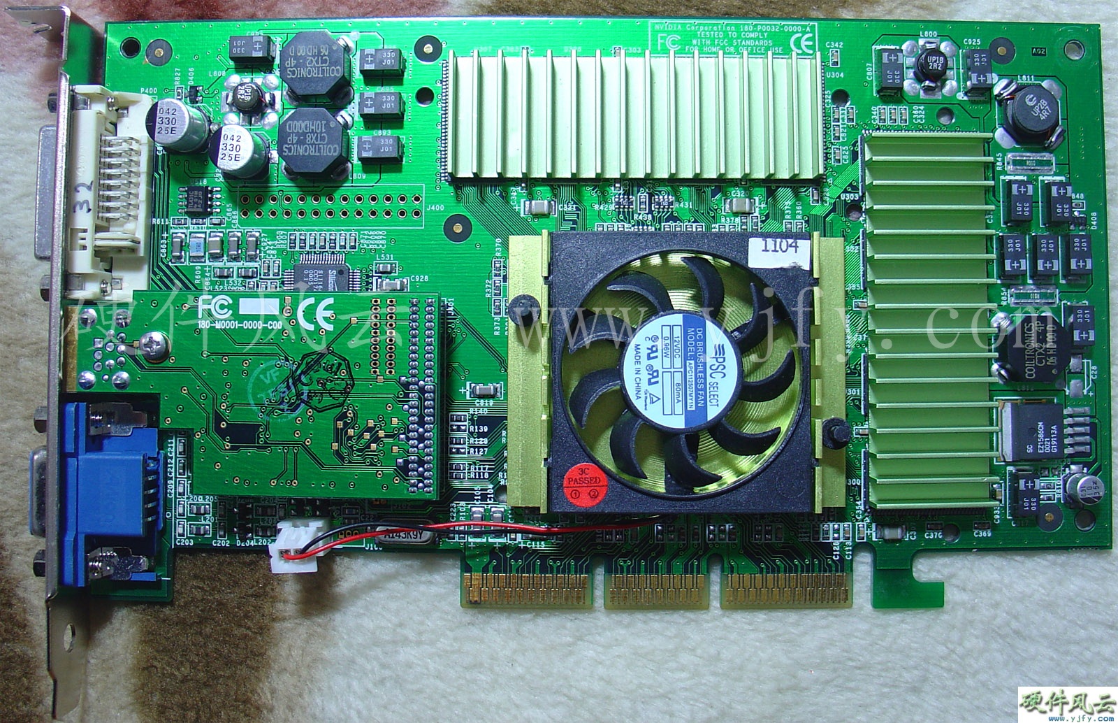
GeForce FX5800 Ultra Engineering
sample
GeForce FX֮�����á�FX�����������֡�5����ԭ��֮һ��nVIDIA�չ�������3dfx����ʦ��������GeForce
FX�Ŀ��������ڴ��µ����δ������ʵ�֣��Լ�GDDR2�Դ�IJ����ƣ����GeForce FX5800/5800 Ultra�Կ���������������ǿʤ��2002������ͷ��Radeon
9700 Pro��R300ϵ������
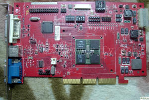
2003��3��6����ATi������Radeon 9800 Pro��ϵ��Radeon
9700 Pro�����Ż�������Ƶ�ʲ��ܺܺõ�֧��GDDR2�İ汾����������GeForce
FX5800 Ultra�Կ����ա�
Radeon 9800 Pro

��From ixbt.com��
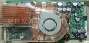
Radeon 9800 Pro���nVIDIA���ֲ�����ֻ����ʱ�����������GDDR2�Դ棬��2003��5��12�շ�����ʹ��GDDR1�Դ��GeForce
FX5900 Ultra��ͼ��������ɢ�Ⱥ��ĵȷ�������ĸĽ�ʹ�ø߶�ϵ��GeForce FX5900 Ultra/FX5950 Ultra������
Radeon 9800 Pro/9800 XT�Կ����⡣
2003 �� 6 �� 13 ��SiS �³������ӹ�˾ Xabre Graphics (XGI)
��δ�����ļ۸��չ���Trident��ͼ��оƬ����ҵ��2003 �� 9 �� 15 �գ�XGI
������Volari V3/V5/V8оƬ�Կ���˫��ʾоƬ�� Volari
Duo V8 Ultra�Կ�������Volari V3�Կ�����Trident XP5�Կ����ƶ����Volari XP5��Volari
Duo V8 Ultra�Կ����ܱ�GeForce FX 5700
Ultra�Ըߣ��������١�������˫��ʾ������͵��������Σ����ڳ�Ϊ�ղصij����
Volari Duo V8 Ultra Engineering
sample
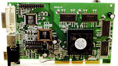
VIA��Chrome��Ʒ�ߵĵڶ�����Ʒ��DeltaChrome S8��DeltaChrome
S8���з���˳��2003��8��S3�������DeltaChrome S8�������壬ֱ��2004��7��28�ղ���ʽ��������֧ԮDirectX
9a��3D���������ѽӽ���ʱ���н��Կ�FX
5700Ultra��
DeltaChrome S8 Engineering
sample

��From legitreviews.com��
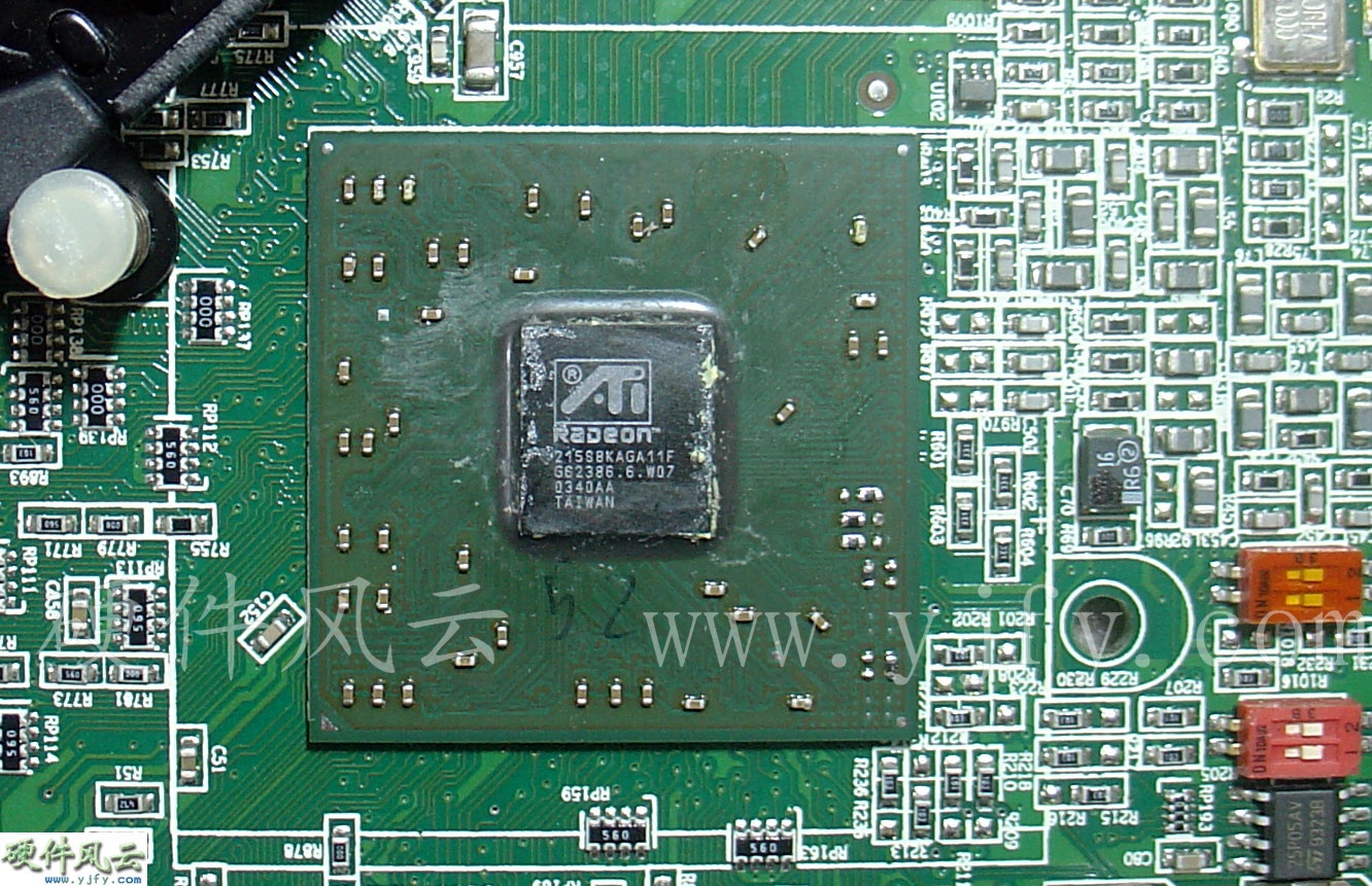
2002��7��23��Intel֧�ֵ�AWG��Arapahoe
Work Group����ʽ����PCI Express���������PCI-E���ٷ����PCIe������ATi��Intel���к�����������2003��9��19�գ�0338�ܣ���IDF2003�ϣ�չʾҵ���һ�����PCI
Express���Կ���δ�����˿��ľ����ͺš�ͼ����ʾоƬ��עΪ��215S8KAGA11F�����Ѽ���PCI-E����RV380��X600���Ĺ�����ƷоƬ���ɼ�ҵ���һ�����PCI
Express���Կ�����Radeon
X600��PCB������0330�ܣ�Լ2003��7����Ѯ����
Radeon
X600
Engineering sample

��PCI
Express�ӿڱ�������nVIDIA
���з������ͺ���Ӧ�Է�������Ƴ�AGP-to-PCI Express�Ž�оƬBR02��BR02ȫ��Bridge
Revision 02�����ΪHigh Speed Interconnect��HSI���������Խ�AGP�ź�תΪPCI-E�źţ���ɽ�PCI-E�ź�תΪAGP�źš�2004��2��17�գ�0408�ܣ�nVIDIA �����˲���BR02оƬGeForce
PCX ϵ���Կ���ͼ�е�BR02-A1 ESоƬ����0345�ܣ����Ǹ��ܵ�ATi��ѹ�������ٶ��͡�BR02-A2
ESоƬ����0407�ܣ�������A2���͡�
GeForce PCX5300
Engineering sample
GeForce PCX��Ҫ���ڲ����ɹ��ľɲ�ƷGeForce
FXϵ�У�����ͨ����ת��Ч�ܸ�������ʧ�����Խ���оƬ����������ATi��Ų����������·������š�����GeForce 6��GeForce
7ʱ�ڣ�BR02оƬ�������������ֳ�������ֻҪ����һ�ֽӿڵ�оƬ��ATiоƬ��Ϊԭ������һ��оƬͬʱ�Ƴ�ԭ��PCI-E��ԭ��AGP�汾��������ڳɱ�ѹ�������PCI-EѶ��תΪAGP��Rialto�������оƬ��
nVIDIA��̨ʽ����PCI-E�ӿ��Կ������ƿ�����ʹ����2004��5��17�����Ϲ���˶��γ����ͨ�����������ڵ�10��̨��ʼDZ����Գ��̣���������ԱʼDZ����Ե��ƶ�PCI
Expressģ��(MXM)���MXM����ȫ��ΪMobile PCI eXpress Module��
GeForce PCX5300 MXM Engineering sample
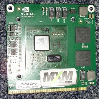
(From hexus.net)
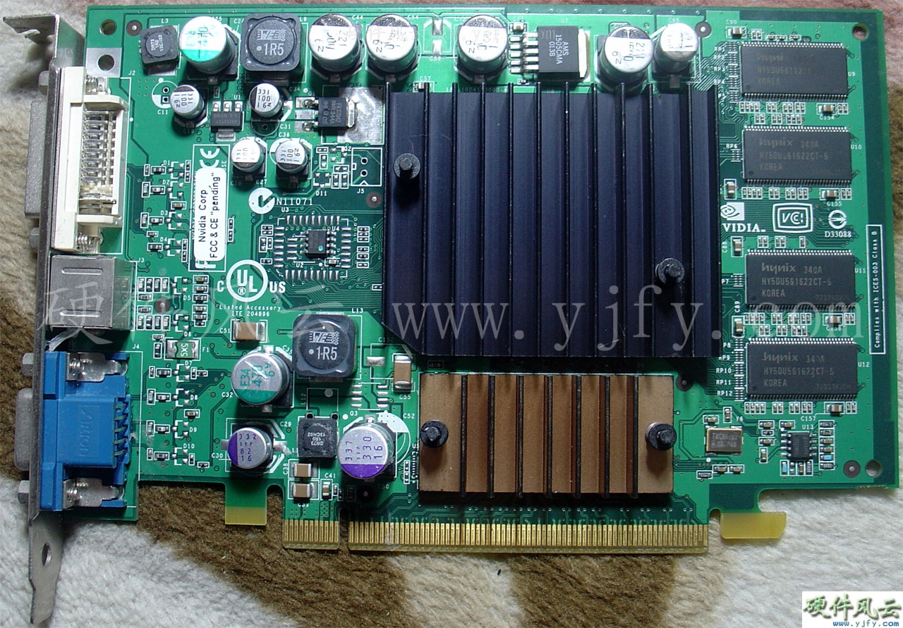
nVIDIA �������� GeForce FX �����ż����ж˰汾���ж˵� FX5600 (NV31)��FX5700
(NV36)�����ż� FX5200/5500/5100 (NV34)���Լ���Ӧ���ƶ��档
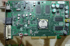
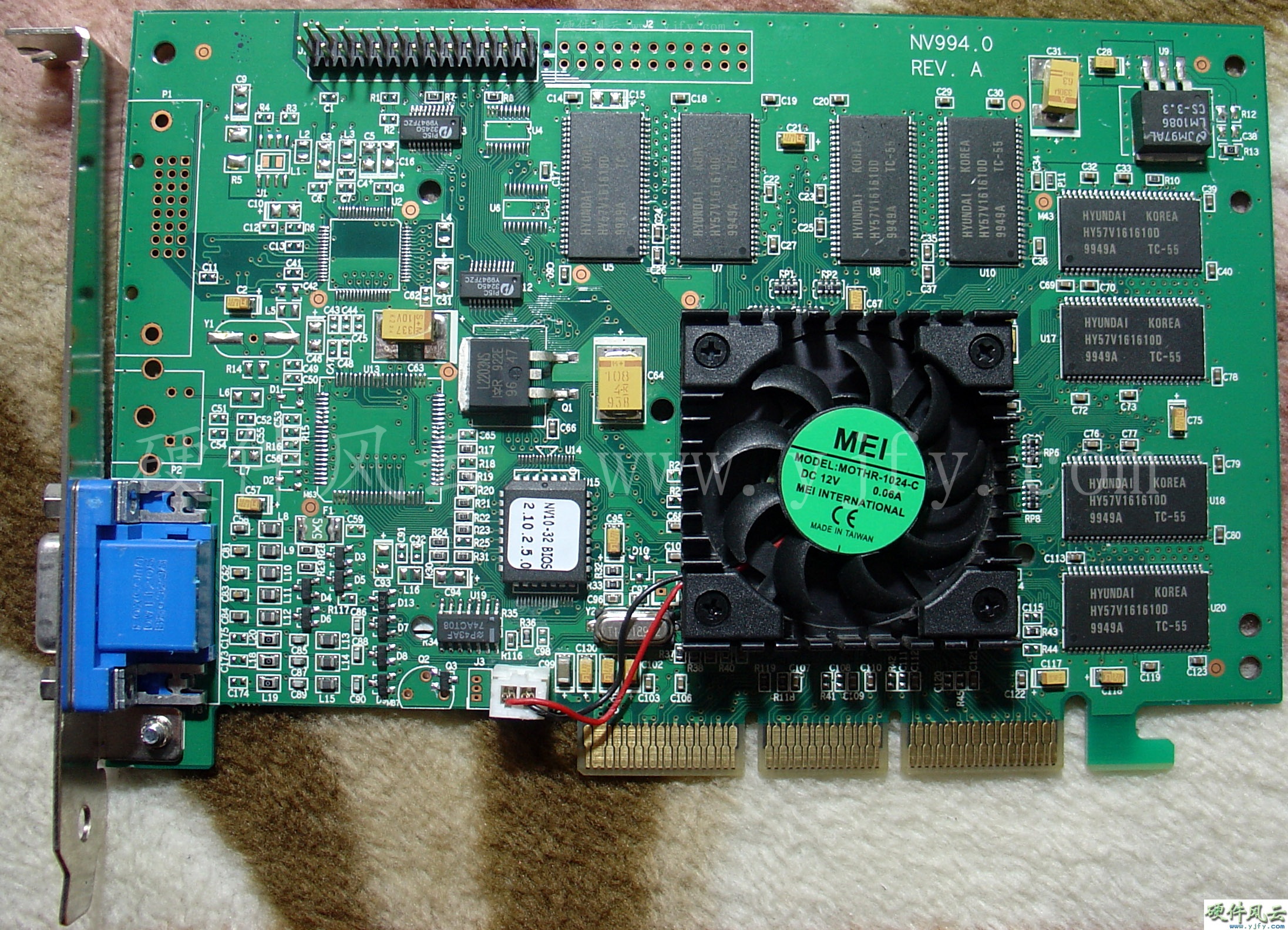
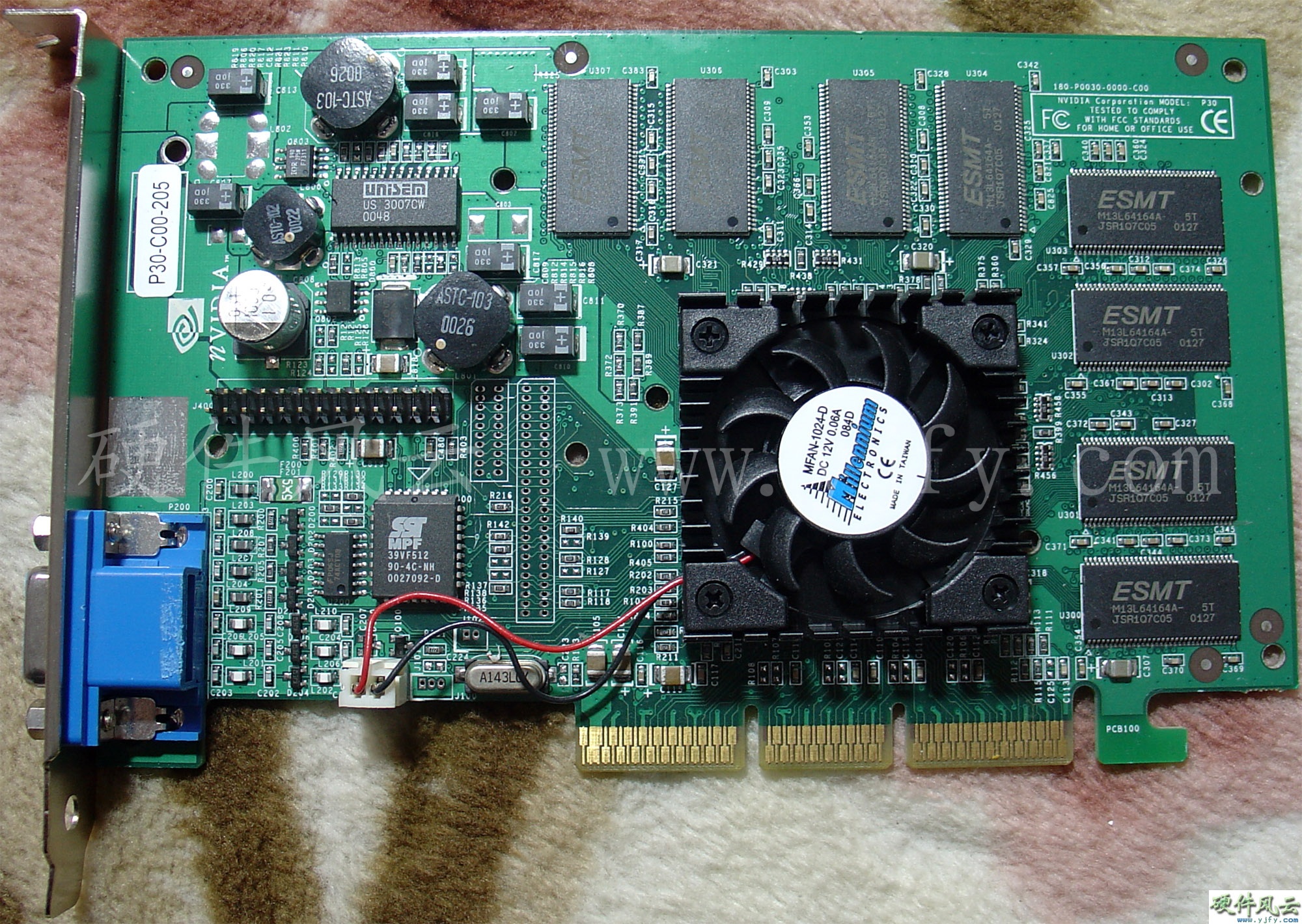
5.1
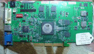
GeForce FX5800/FX5800 Ultra
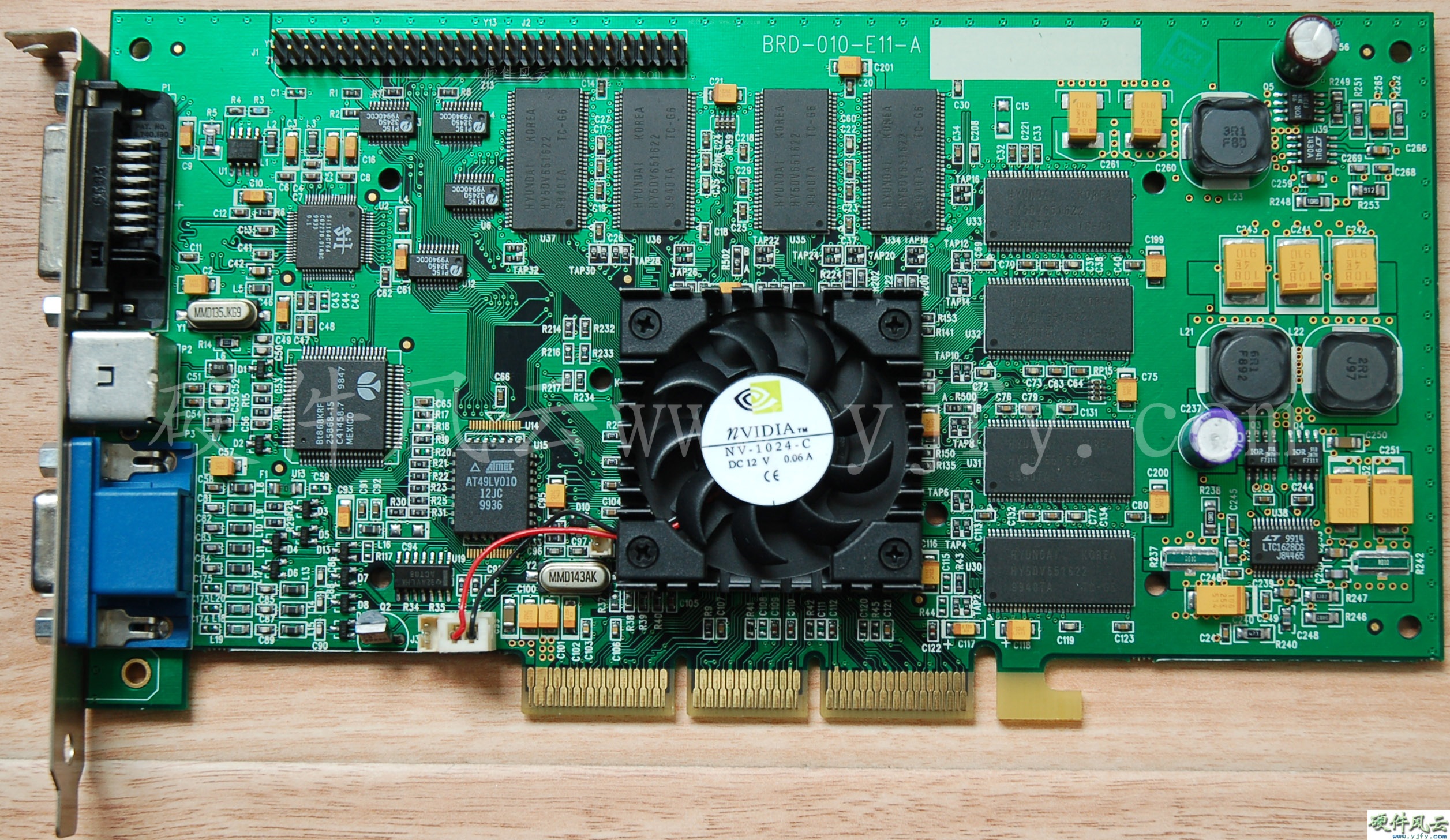
5.1.1 Rev A00
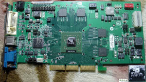
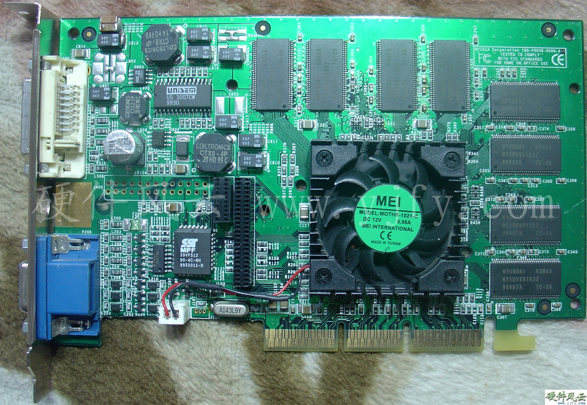
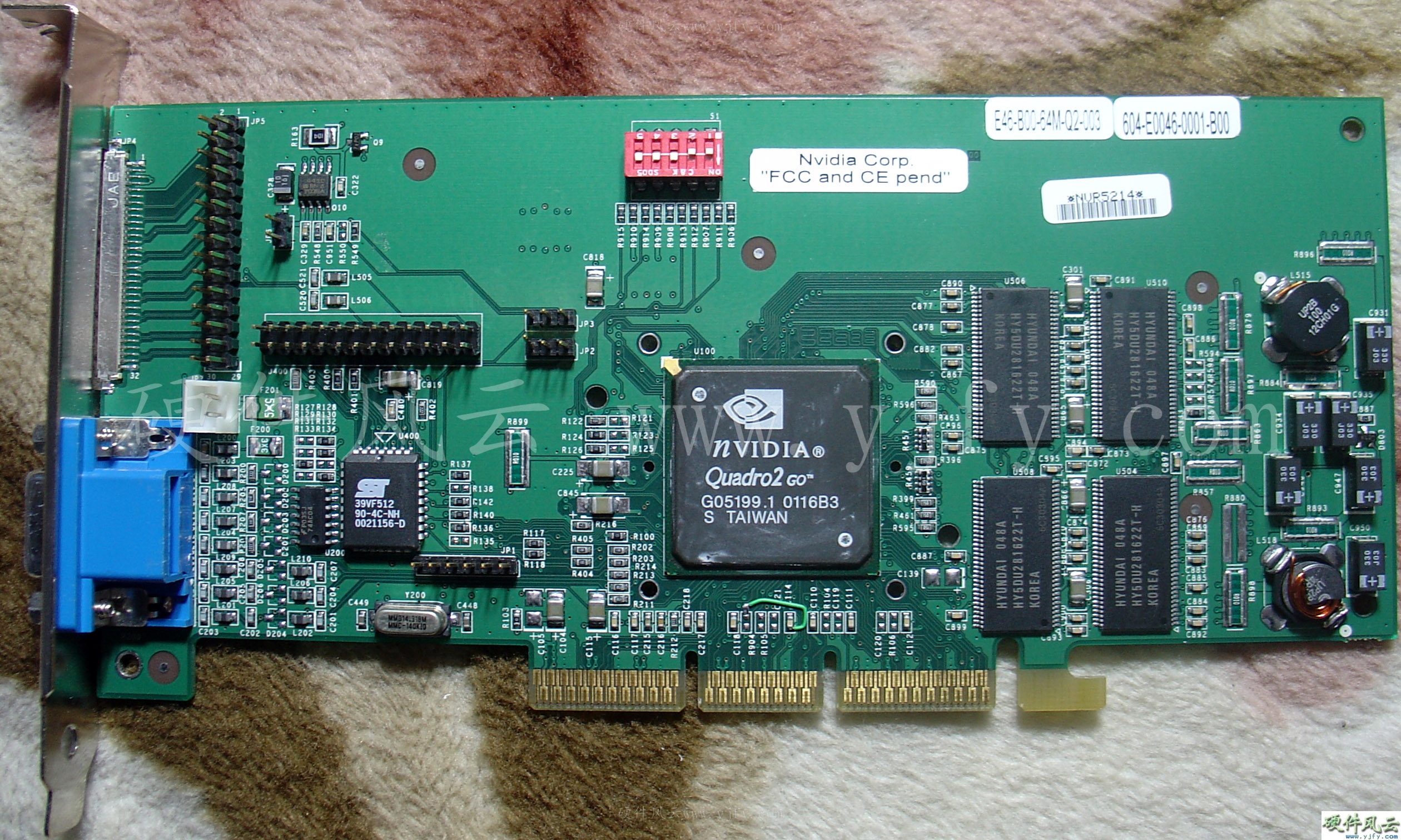
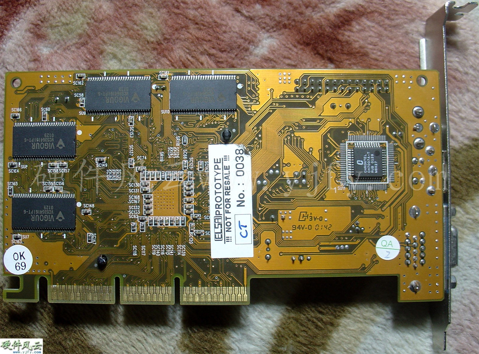
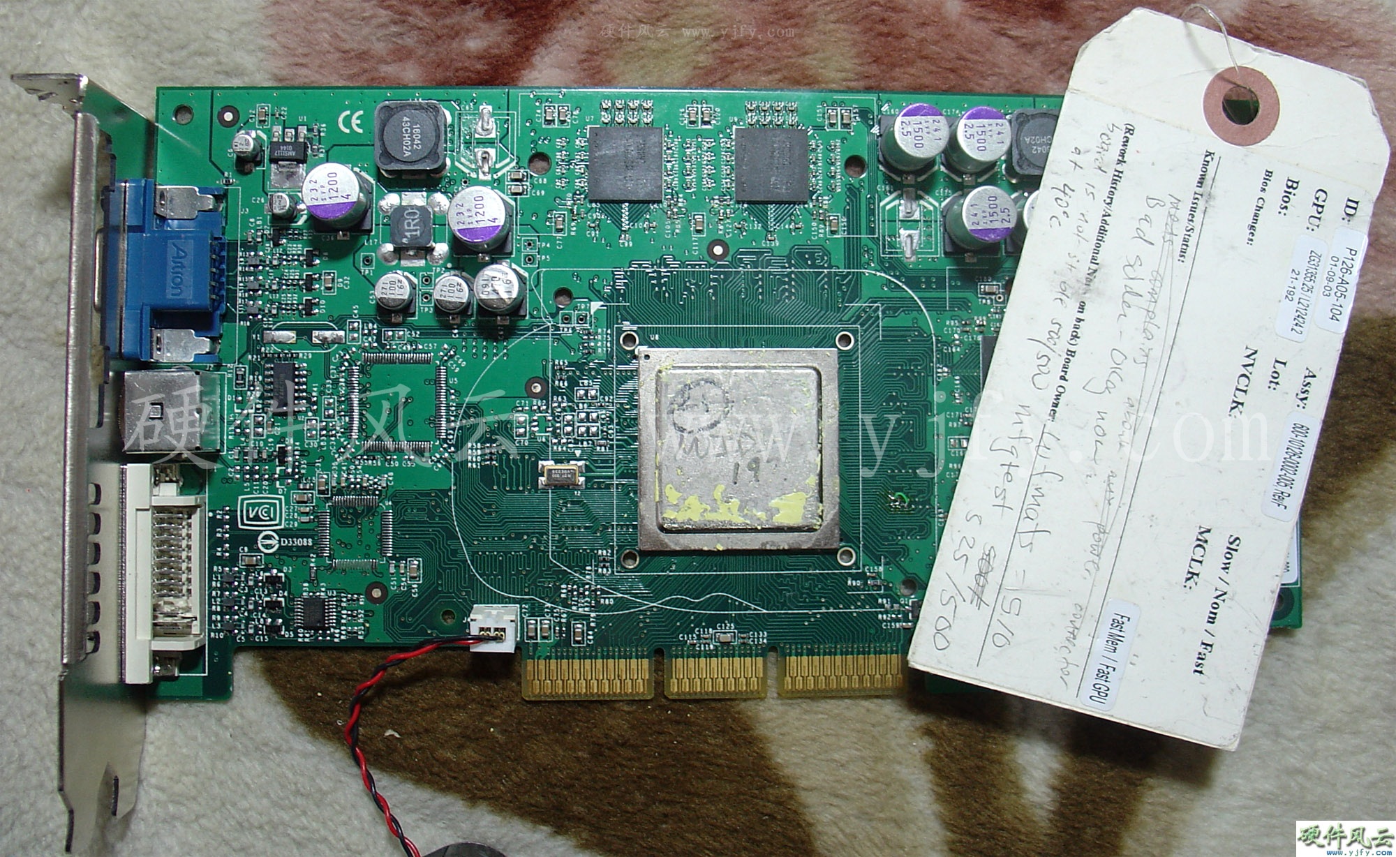
GeForce FX��Rev A00�����֣�ʹ��GDDR1�Դ��T01��ʹ��GDDR2��P126��T01��P126�����濴δ�����𣬽���T01���õ�����С��
5.1.1.1 T01
PCB Code:180-10T01-0000-A00
��һ��
NV30 ��Ƭ�� 2002 �� 8
����Ѯ��Ƭ(0232��)����װоƬԼ��4��(0236��)������оƬԼ��4��(0240��)�����T01��PCB������0240��Ҳ�����ν��ϣ�PCB����NV30оƬ��������װ��оƬ,оƬ��ע���£�
TMG177-12"-PI8124��12
inch wafer��
N91517.06��δ֪��
EHS-FCBGA
1152��External Heat Spreader Flip Chip BGA 1152 Pin��
Ibiden Daisy
Chain��Ibiden Co Ltd ,Daisy Chain Topology��
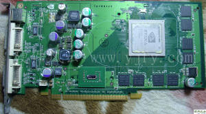
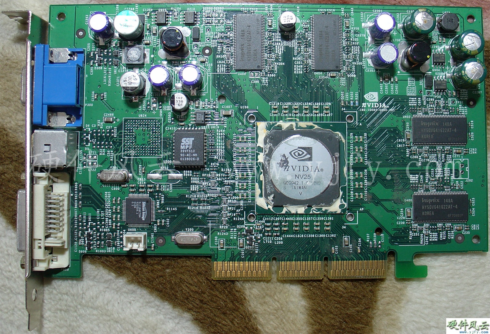
T01��NV30оƬ��оƬ�����壬ʹ�ó���ɿ���MBGA��װ��GDDR1���Դ档��֤���к�ֱ�Ӹ��Ƴ�ʹ��GDDR2�Դ��P126��Ʒ������/�ο��塣
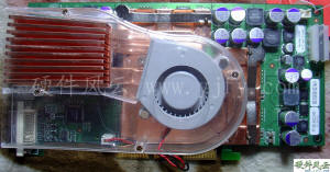
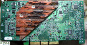
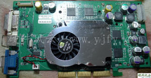
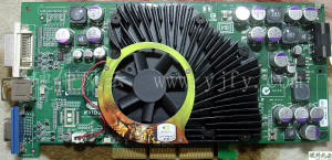
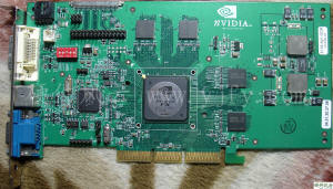
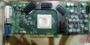
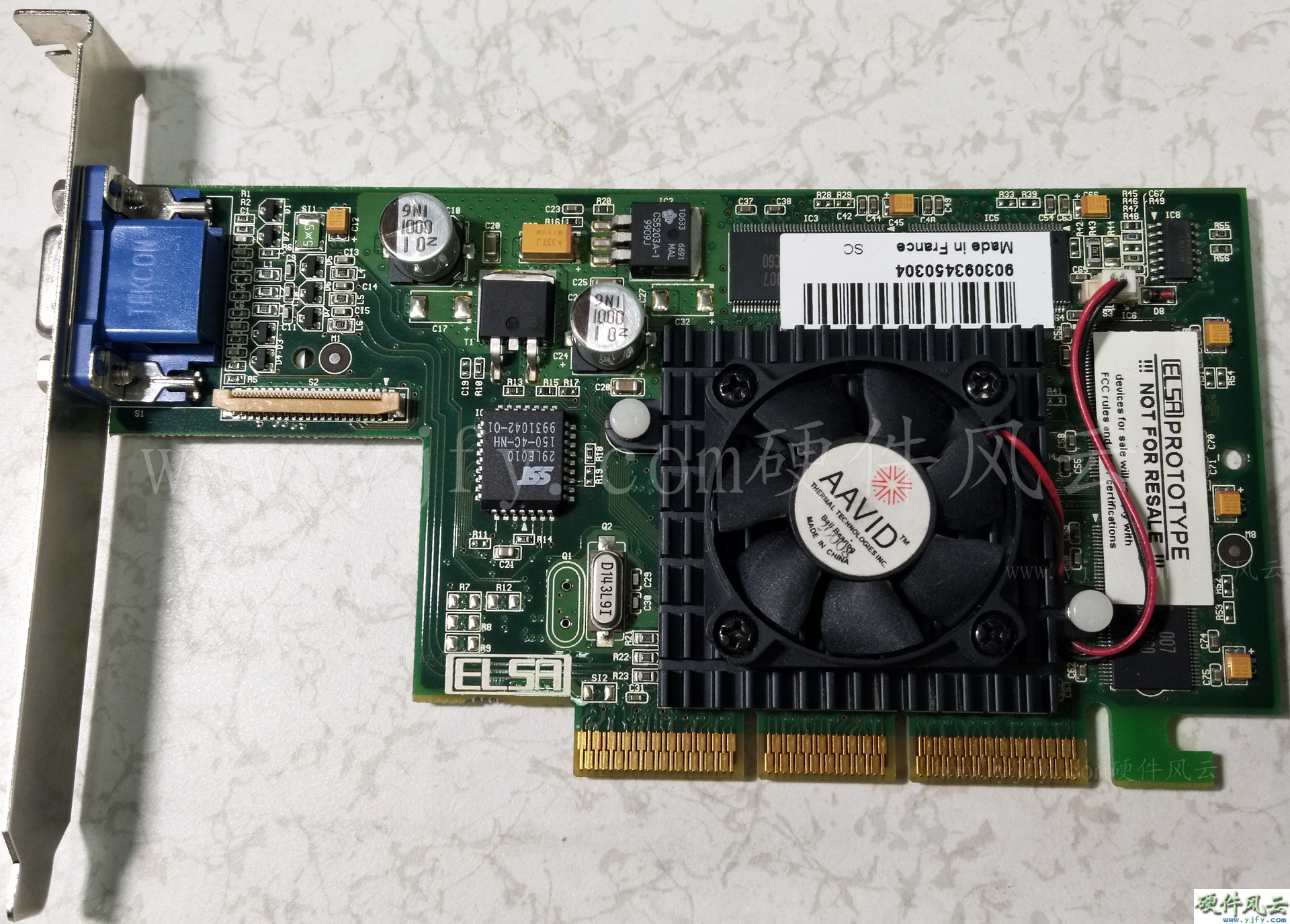
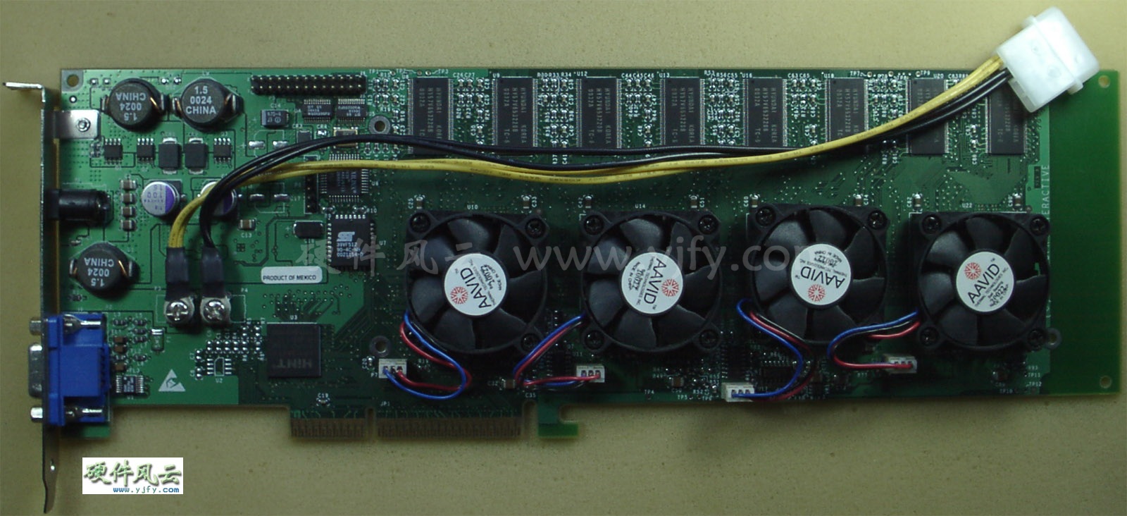
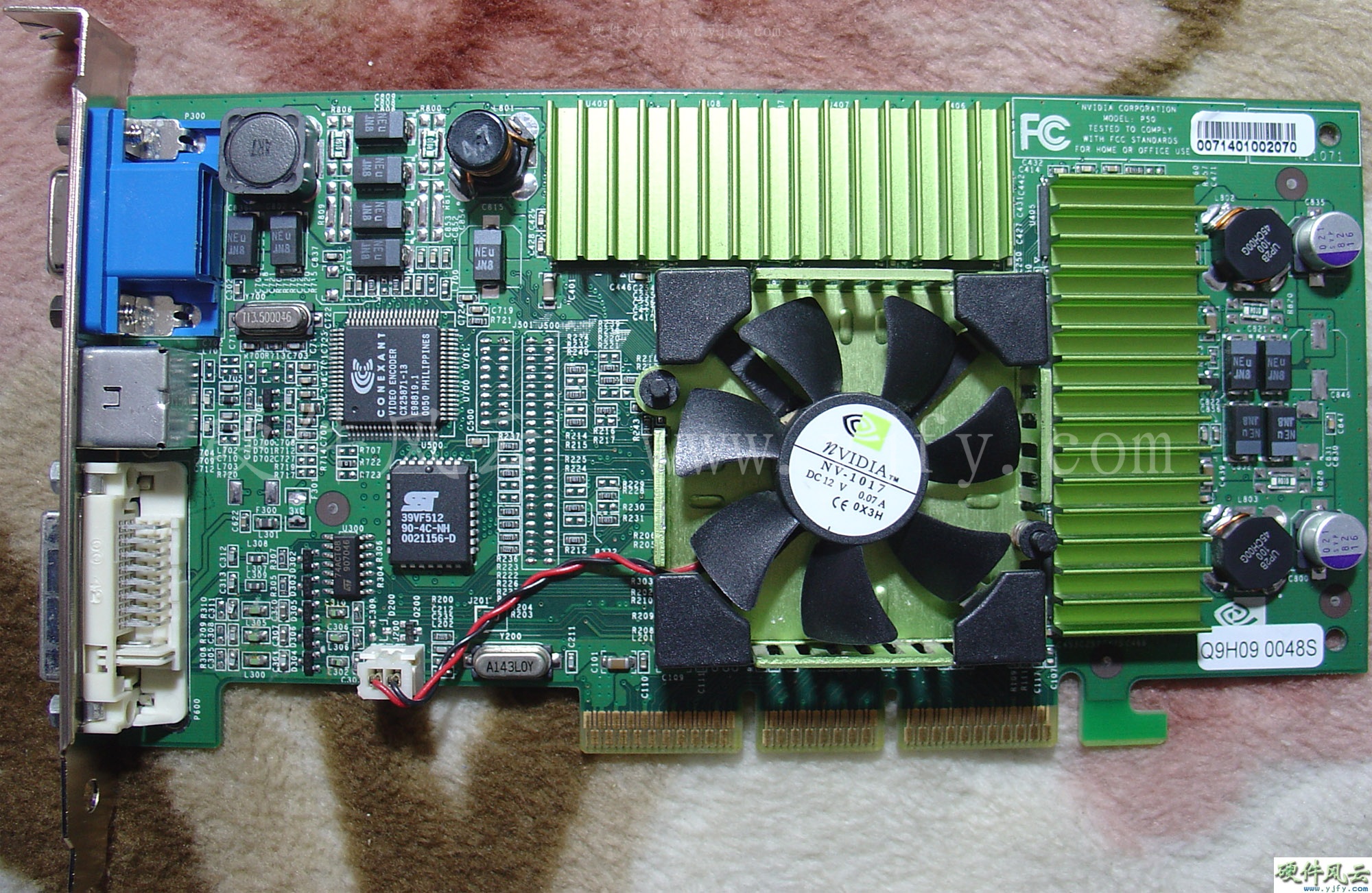
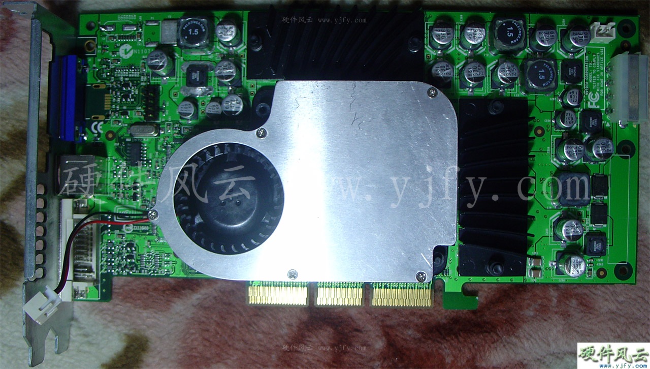
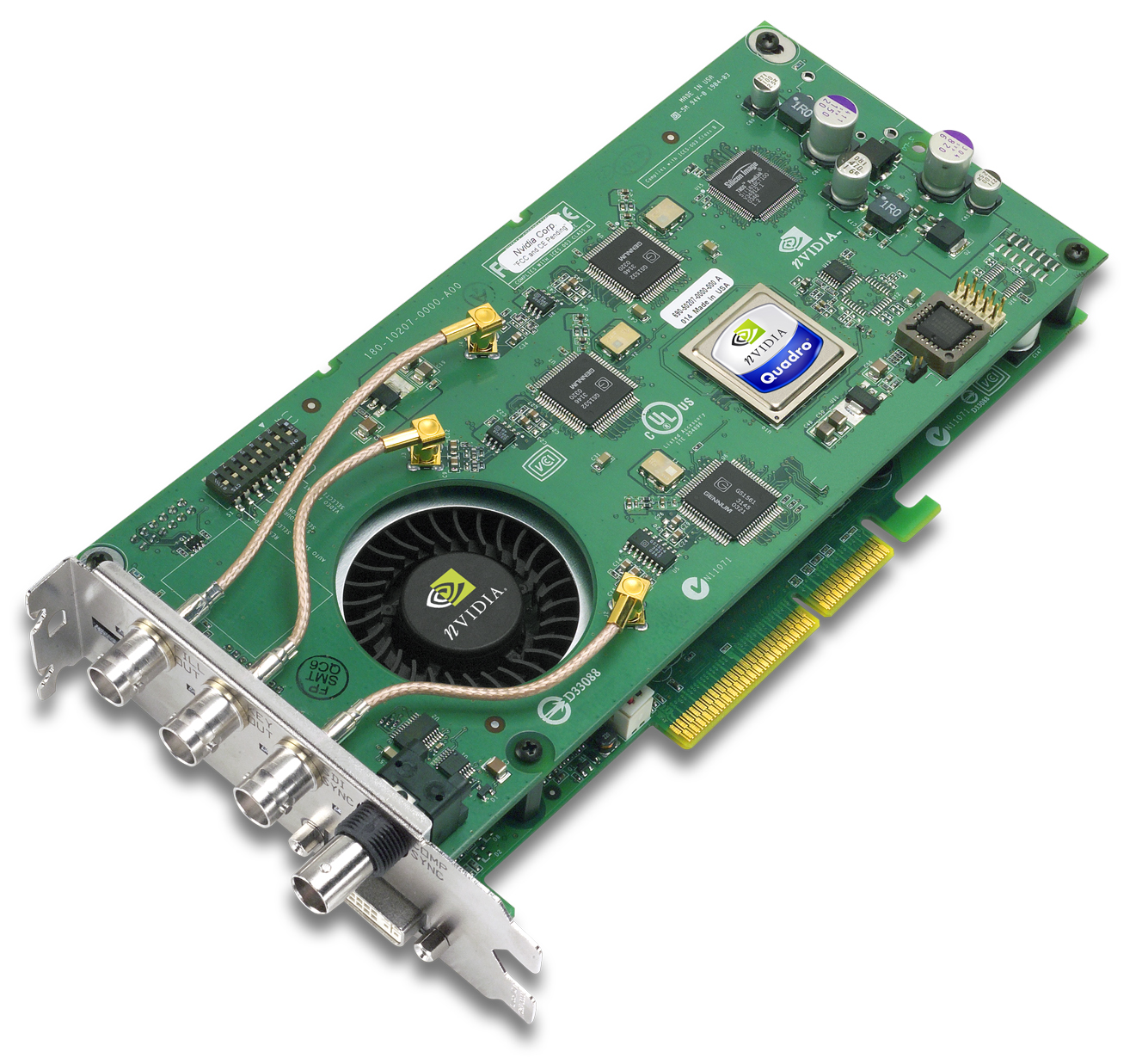
ɢ��ϵͳ��GeForce FX5800��QUADRO
2000��ԭ�ͣ����ȵ�Դ�������½ǣ����Ȳ����������ϽDz��������½Dz����ֱ�ɢ��Ƭ�ڵ������ý�ˮճ�������½Ƿ��Ȳ���������3���״�������չʾ��Ʒ��
GeForce FX5800 Engineering
sample

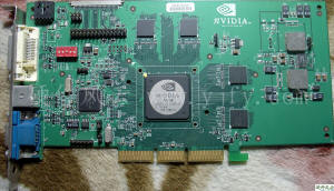
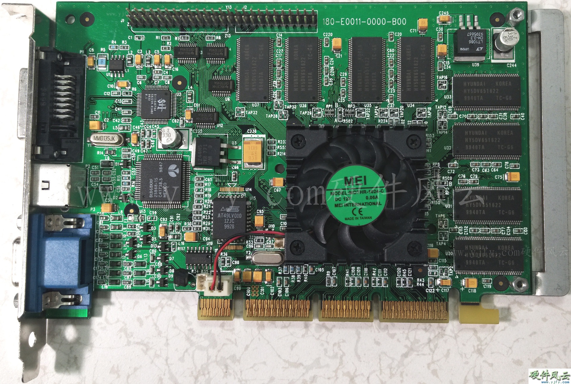
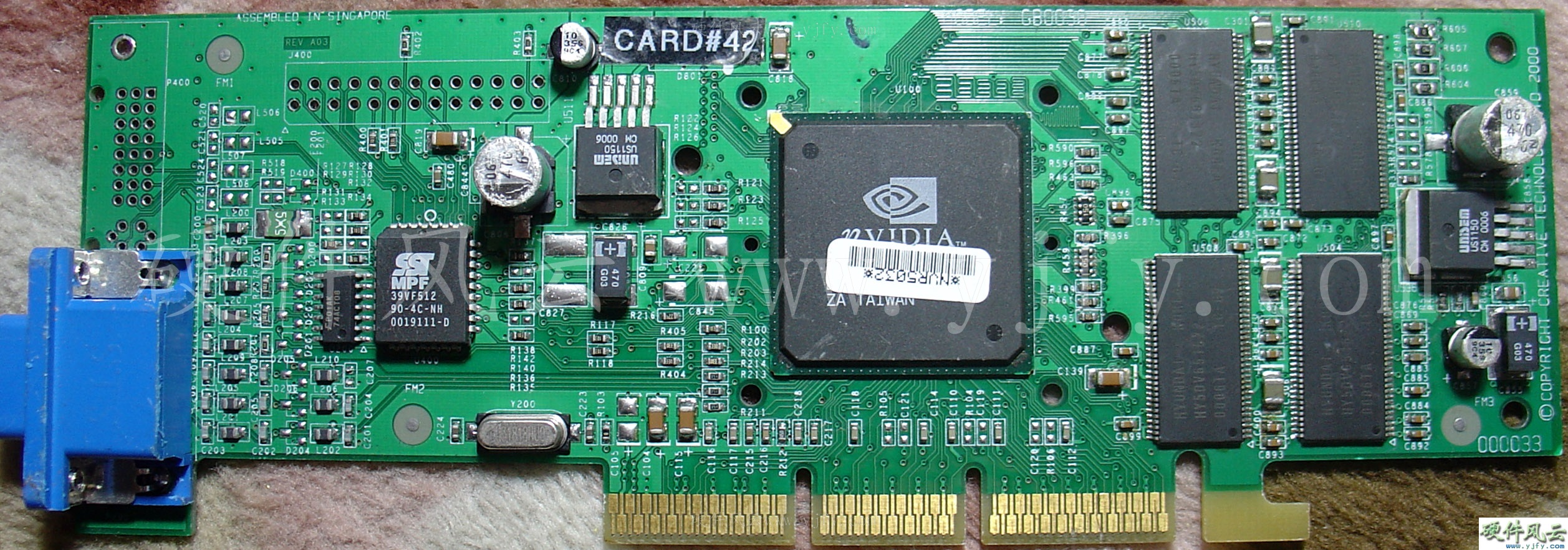
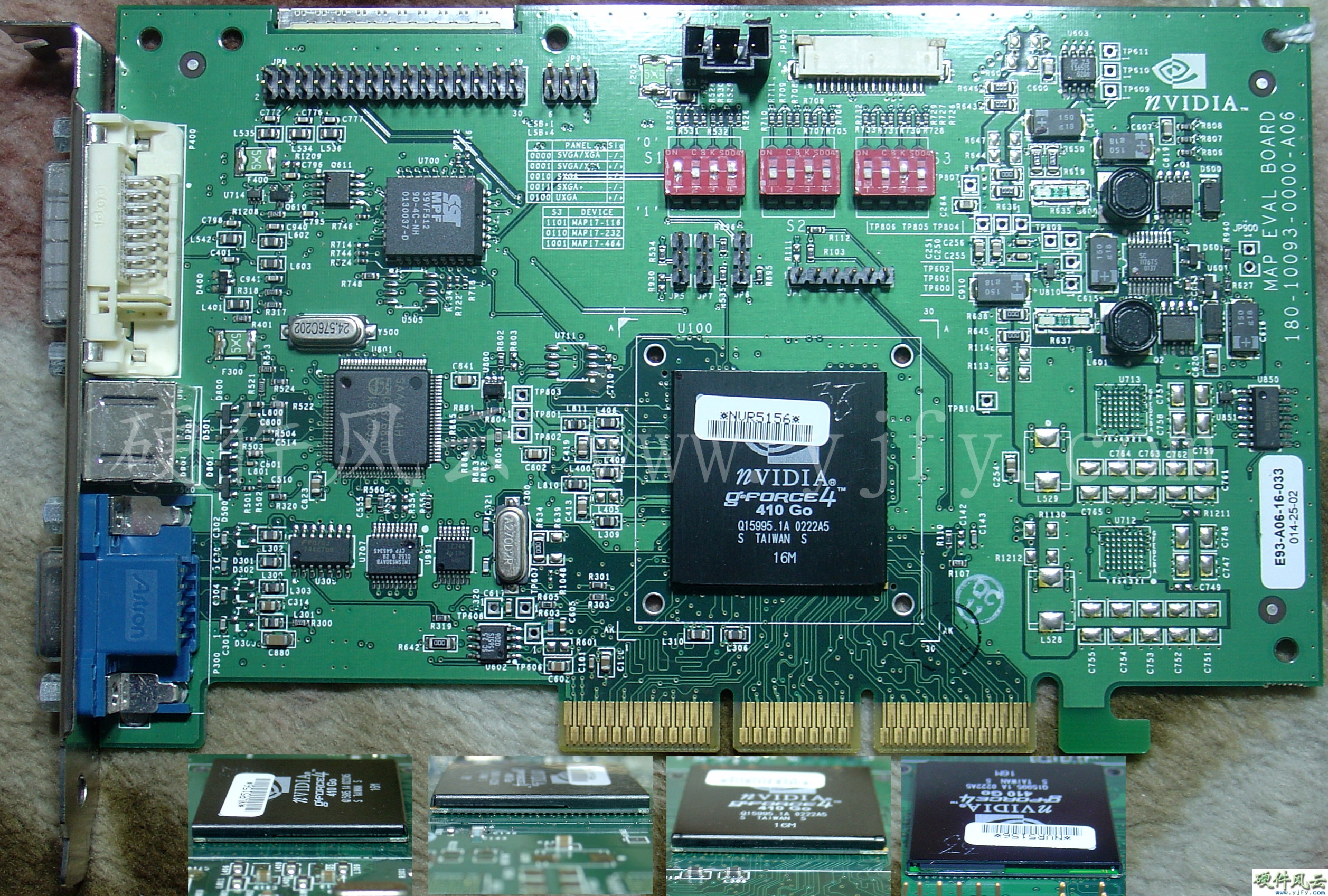
5.1.1.2 P126
��������2002��7��������GDDR2��nVIDIA GeForce FX����һ��ʹ��GDDR2���Կ�����2002��11��18�գ�0247�ܣ���COMDEX2002����GeForce
FX����ʱ��GeForce
FX����ͼƬ�����������ͼƬ��ͼƬ�Ĺ�����Ʒ���ϵ������Դ����ΪES�汾������Ϊ0238�ܡ�PCB����Ӧ��0240��0241�ܡ�
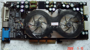
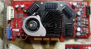
GeForce FX5800 Ultra
Engineering sample
COMDEX2002�ϻ������������ַ��ȵ�GeForce FX���ƺ�����Ƴɱ��Ըߣ���������
GeForce FX5800 Ultra
Engineering sample

��From
ixbtlabs.com��
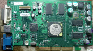
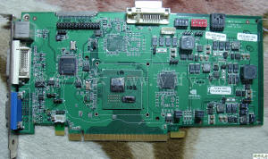
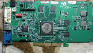
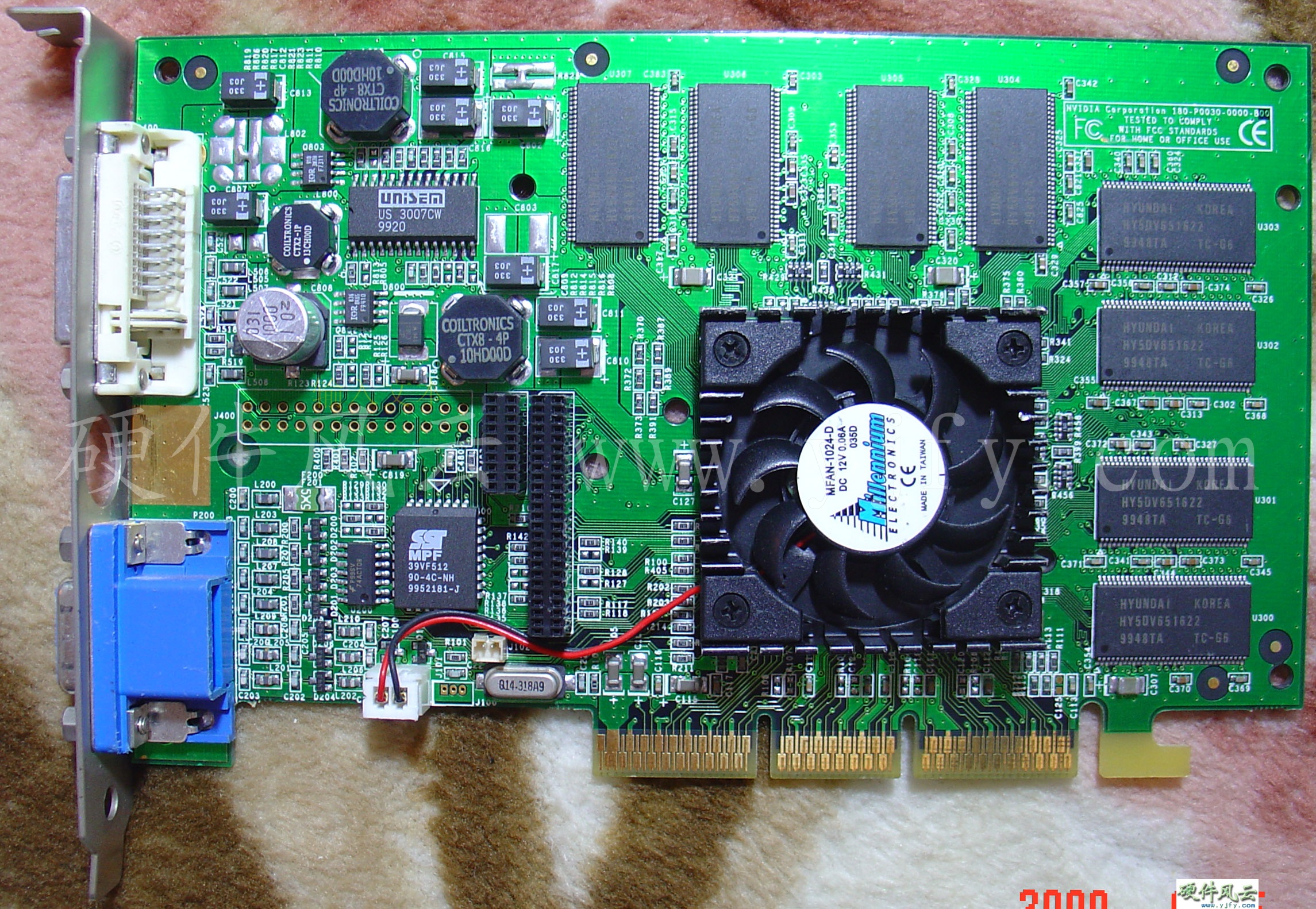
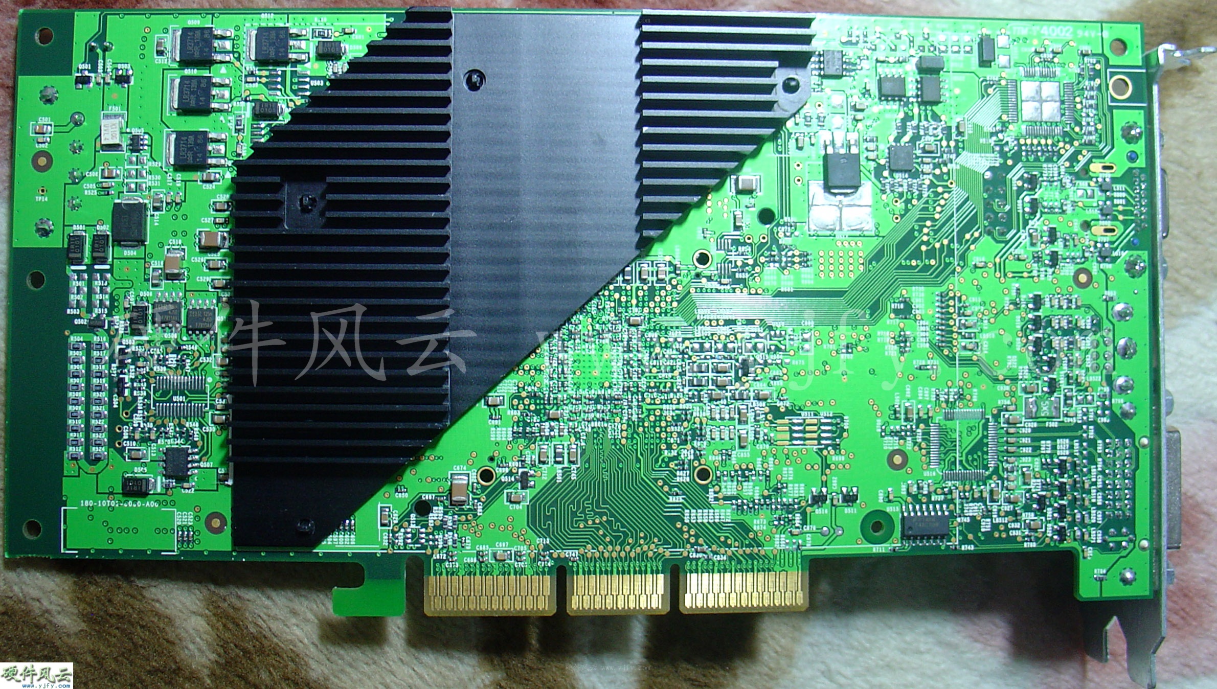
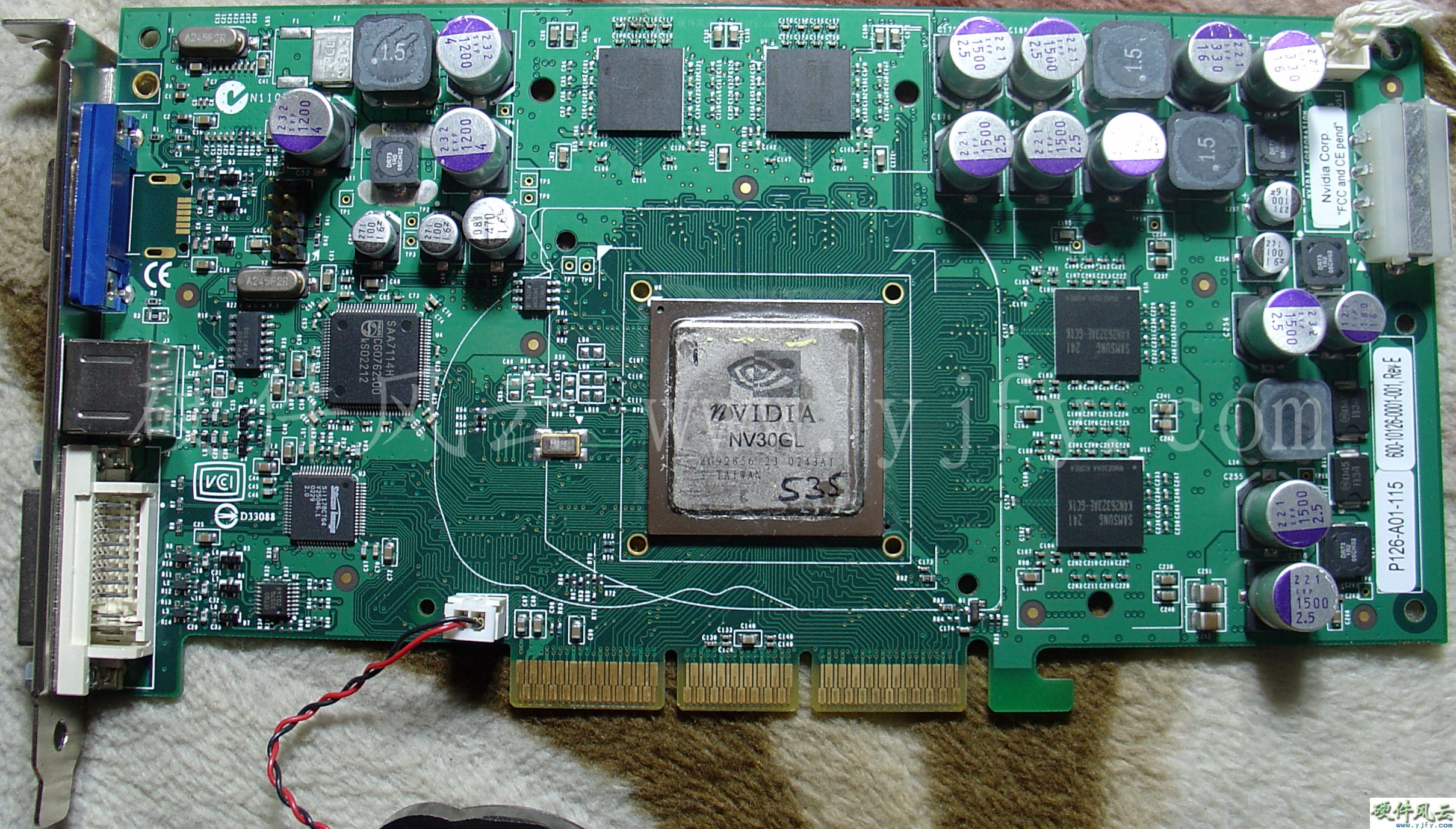
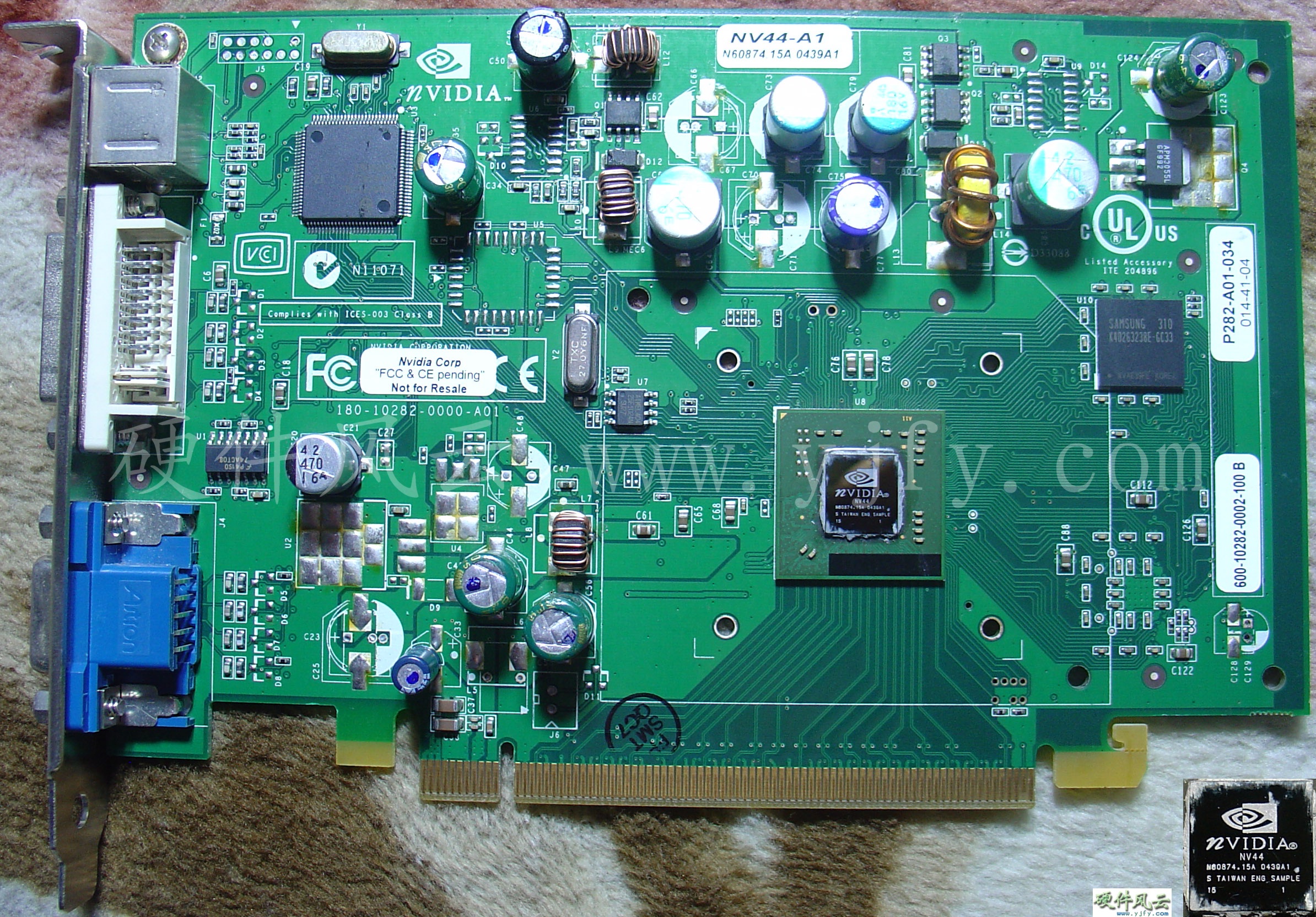
5.1.2 Rev A01
PCB Code:180-10126-0000-A01
Chip model:NV30GL A1
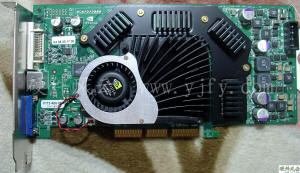
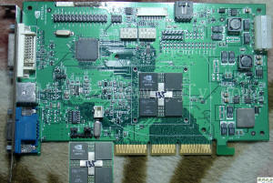
�Դ��������0241�ܣ�������ʽ�档PCB����0242�ܣ�NV30оƬ������0243�ܣ��汾ΪA1��оƬ��Ȼ��עΪNV30GL������δ��QUADRO��GeForce
FX֮�֡���NV30оƬΪA2��ʱ�����ΪGeForce FX��ʾ��ʽ���������ΪQUADRO 2000���ڹ�����Ʒ�Ρ�
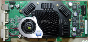
����ɢ��ϵͳ��GeForce
FX��ѡ������ɢ�������ͣ�����Ҫ�����еͶ��Կ���ɢ�ȡ�
GeForce FX5800 Ultra
Engineering sample
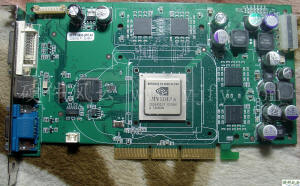
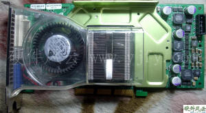
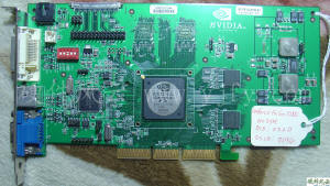
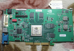
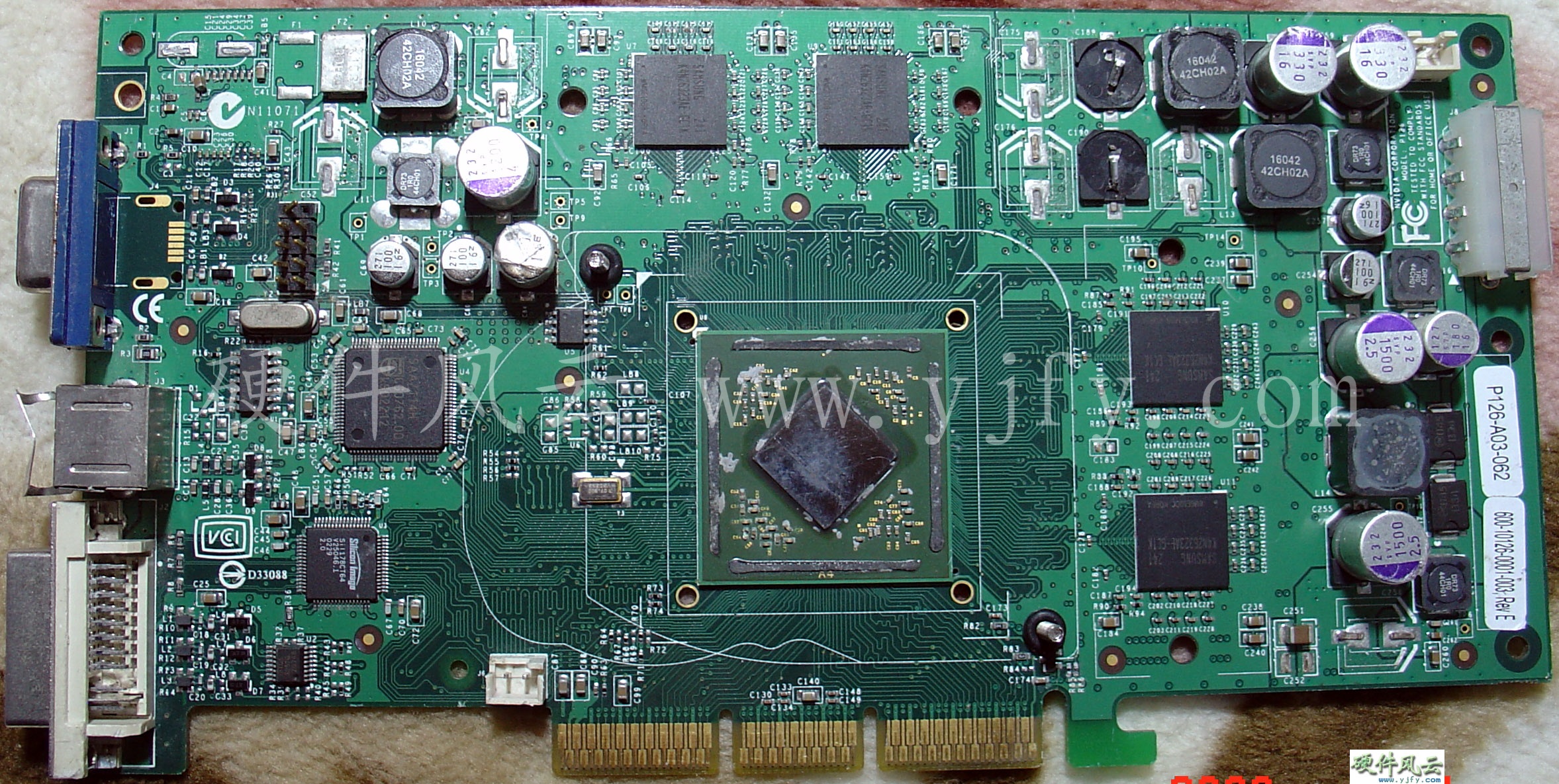
5.1.3 Rev A02
PCB Code:180-10126-0000-A02
Chip model:NV30GL A1
оƬ����0244�ܣ�PCB����0244�ܡ�
ѡ�������ֳɱ��Ե͵�����ɢ������nVIDIA's FX Flow cooling technology�������ձ����á�
GeForce FX5800 Ultra
Engineering sample
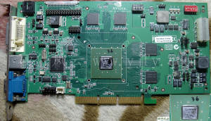
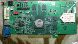
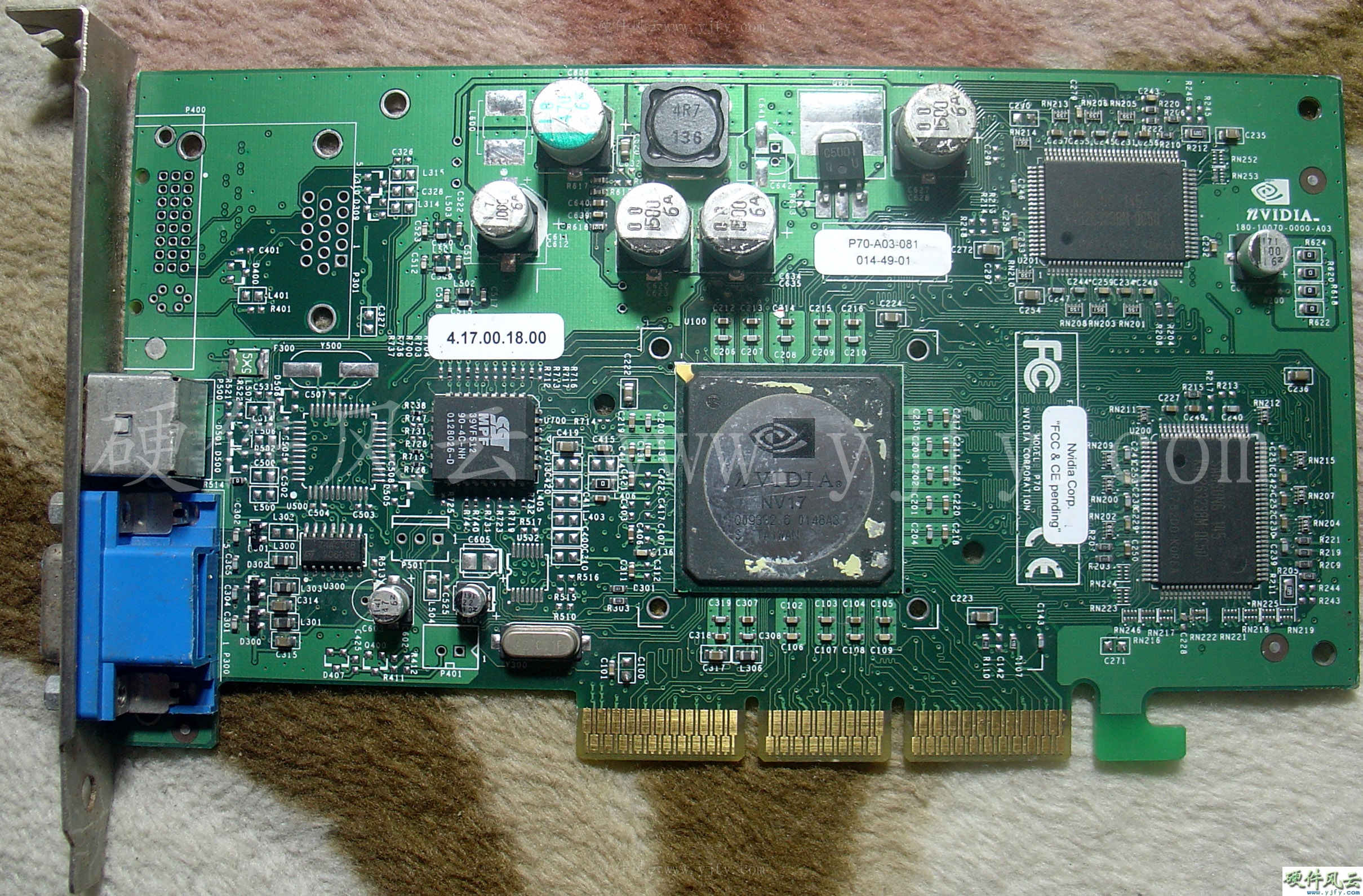
5.1.4 Rev A03
PCB Code:180-10126-0000-A03
PCB����0245����
GeForce FX5800 Ultra
Engineering sample

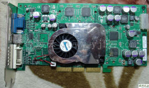
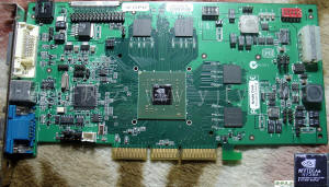
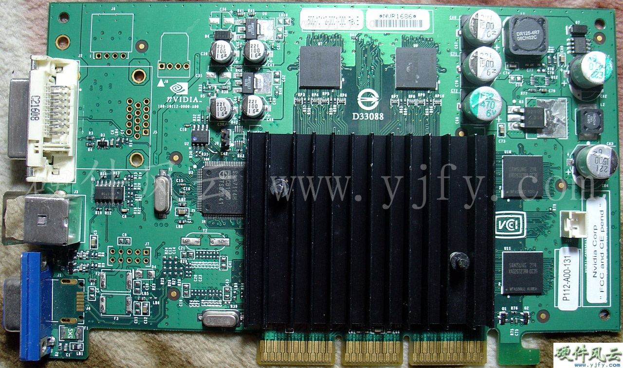
5.1.5 Rev A04
PCB Code:180-10126-0000-A04
PCB����0249����
GeForce FX5800 Ultra
Engineering sample

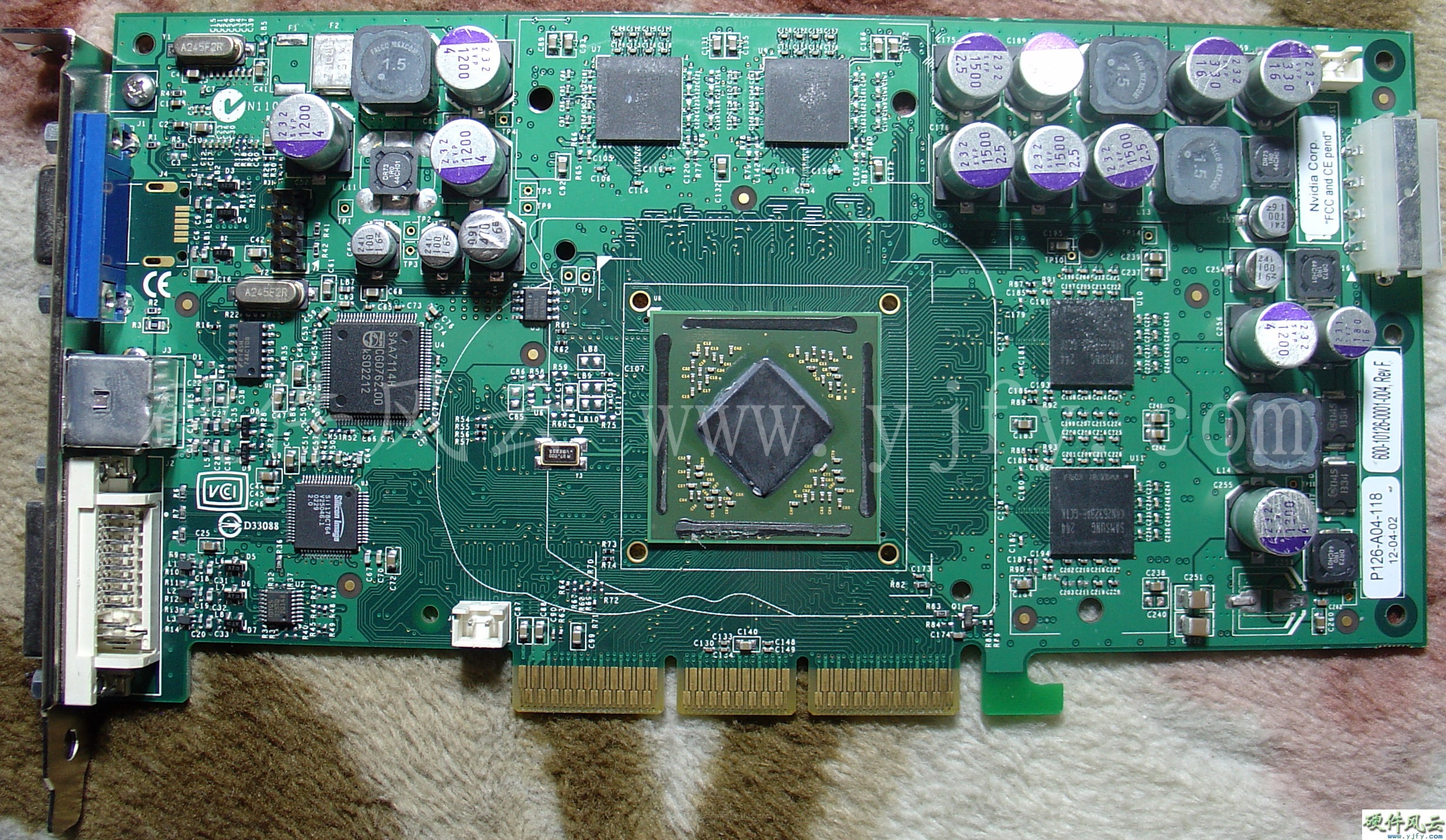
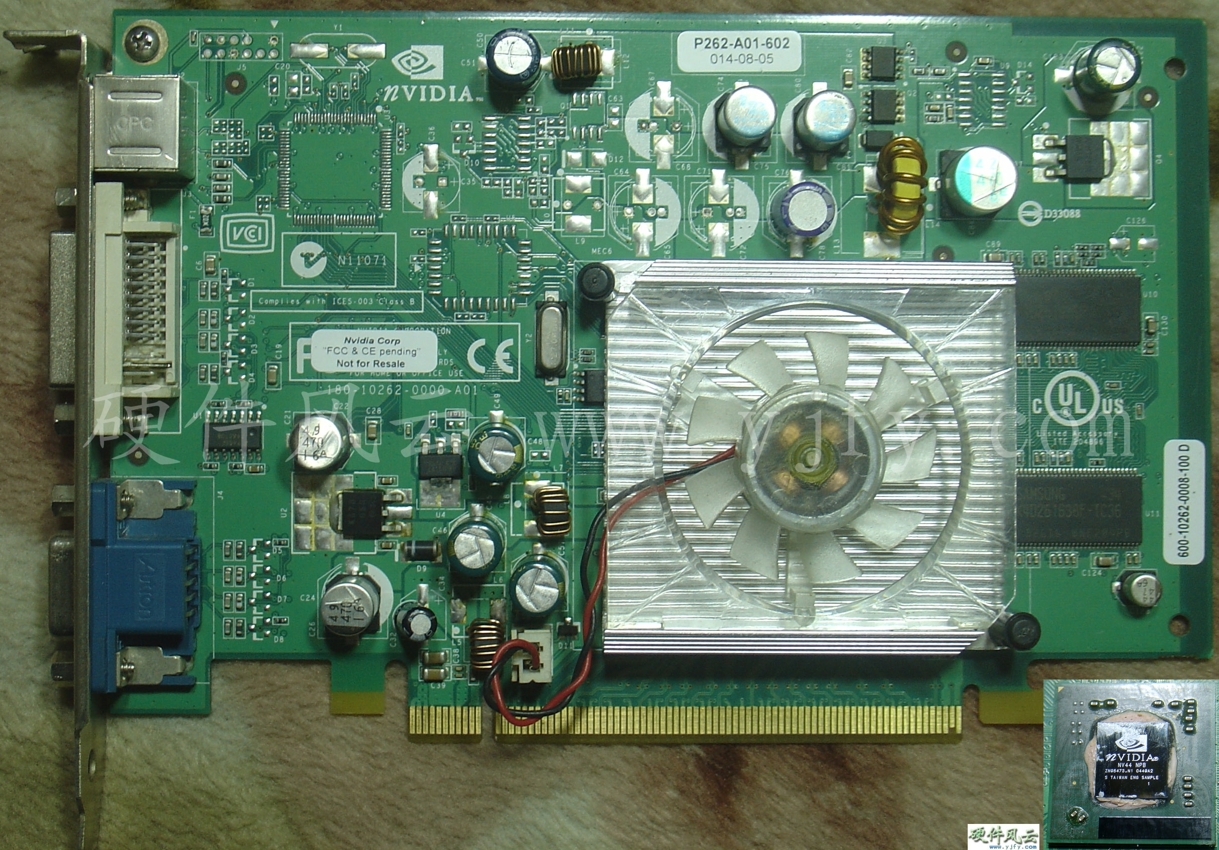
5.1.6 Rev A05
PCB Code:180-10126-0000-A05
PCB����0251����
���������Ķ��ϴ�����ʽ���͡��˿����ڶ�GDDR2�Դ棬����оƬ���ڽ�����Ҫ�IJ��ԣ��ɼ�ֱ�����GeForce
FX5800 Ultra�����ˣ�Ӳ����Ȼ���ڲ������⣬����ʱ�䲻���ˣ�ֻ��Ӳ��ͷƤ�ϣ�Ѻ�������������Ĺ�����ƷPCB������0301�ܡ�
GeForce FX5800 Ultra
Engineering sample


5.2
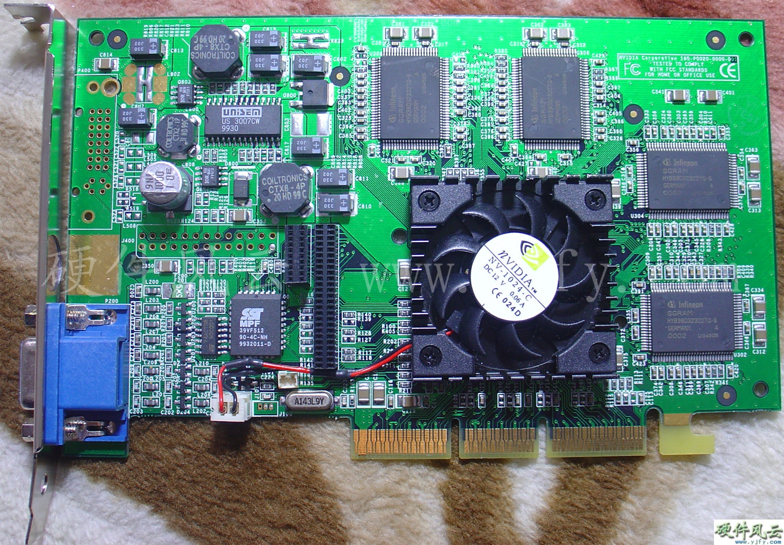
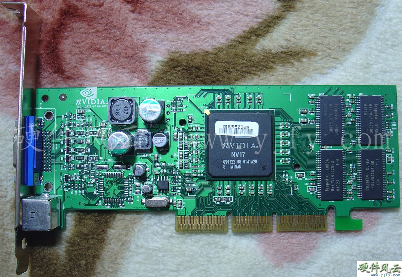
GeForce FX5200/FX5200 Ultra
2003 �� 3 �� 6 ��������
5.2.1 E133
PCB Code:180-10133-0000-A01
Chip model:NV34 A1B2
ES
оƬ����0303�ܣ�PCB����0305�ܡ�
GeForce FX5200 Engineering sample
5.2.2 P162
Chip model:NV34-A2
PCB Code:180-10162-0000-A03
оƬ����0309�ܣ�PCB����0309�ܡ�
GeForce FX5200 Engineering sample
5.2.3 P140
PCB Code:180-10140-0000-A01
Chip model:NV34U A2
оƬ����0309�ܣ�PCB����0309�ܡ�
GeForce FX5200 Ultra Engineering sample
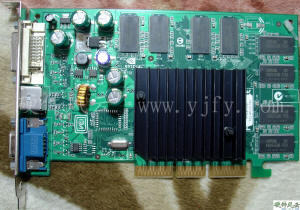
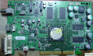
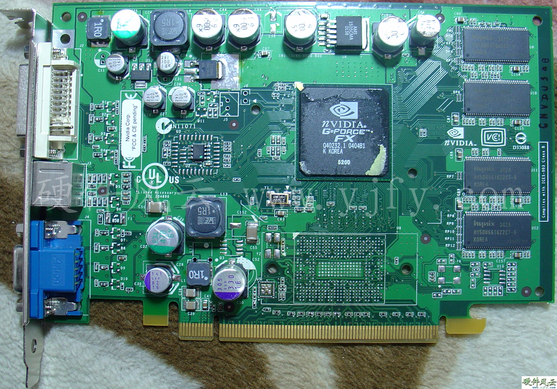
5.3
GeForce FX5600/FX5600 Ultra
2003 �� 3 �� 6 ��������
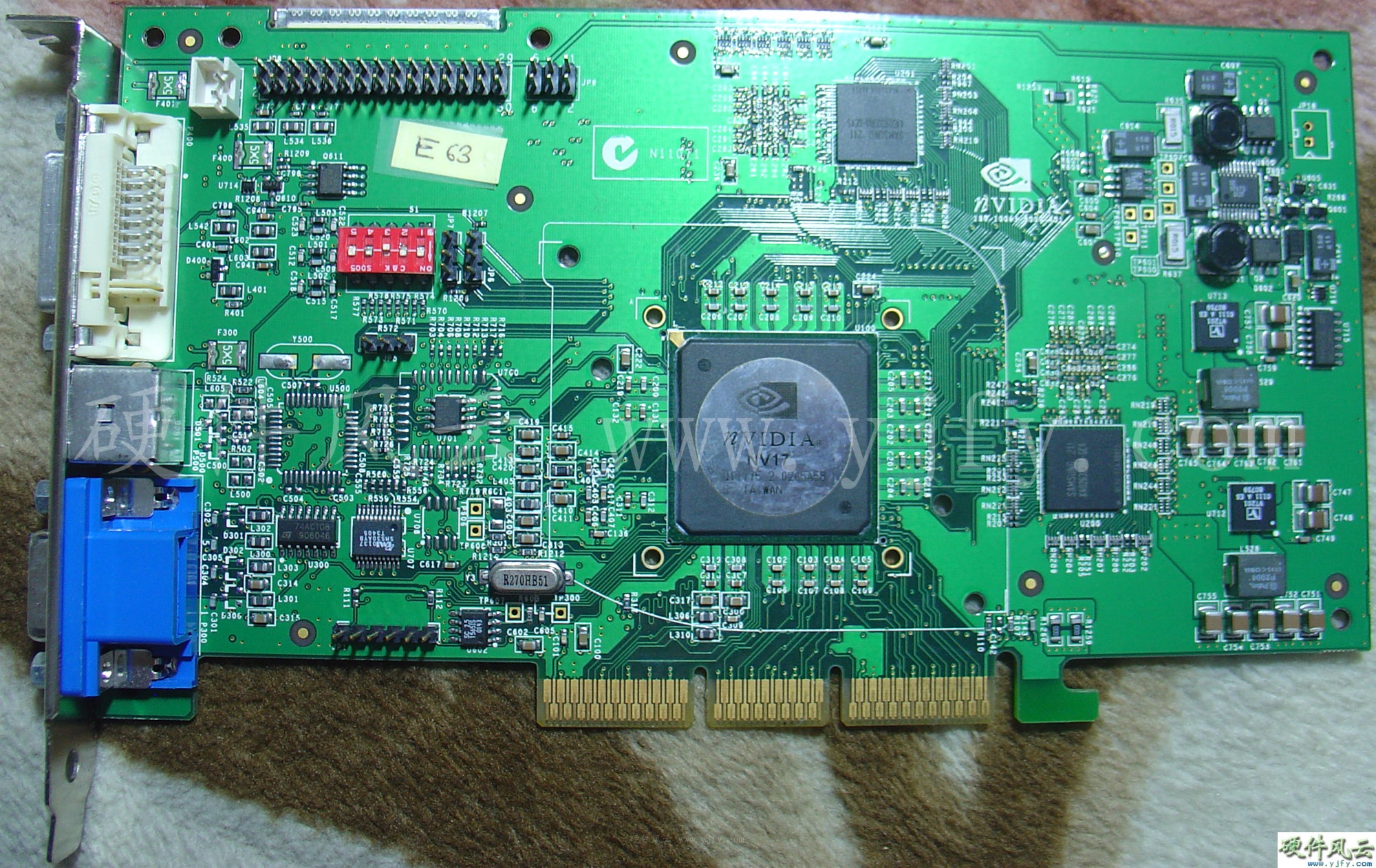
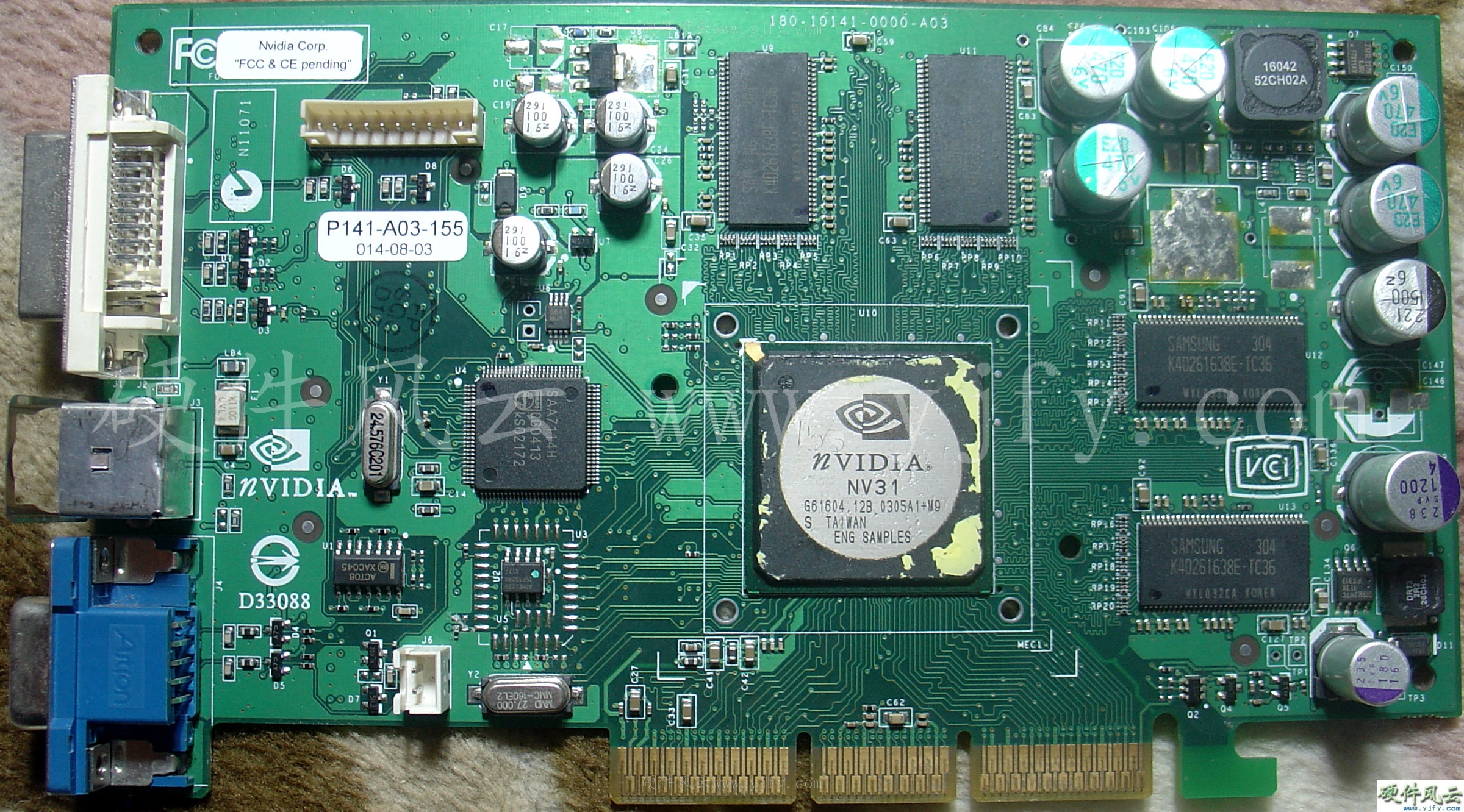
5.3.1 P141
PCB Code:180-10141-0000-A01
Chip model:NV31 A1+M9 ES
оƬ����0305�ܣ�PCB����0309�ܡ�
GeForce FX5600
Engineering sample
5.3.2 P140
Chip model:NV31FC
A1 ES
PCB Code:180-10140-0000-A01
оƬ����0318�ܣ�PCB����0320�ܡ�
GeForce FX5600 Ultra
Engineering sample
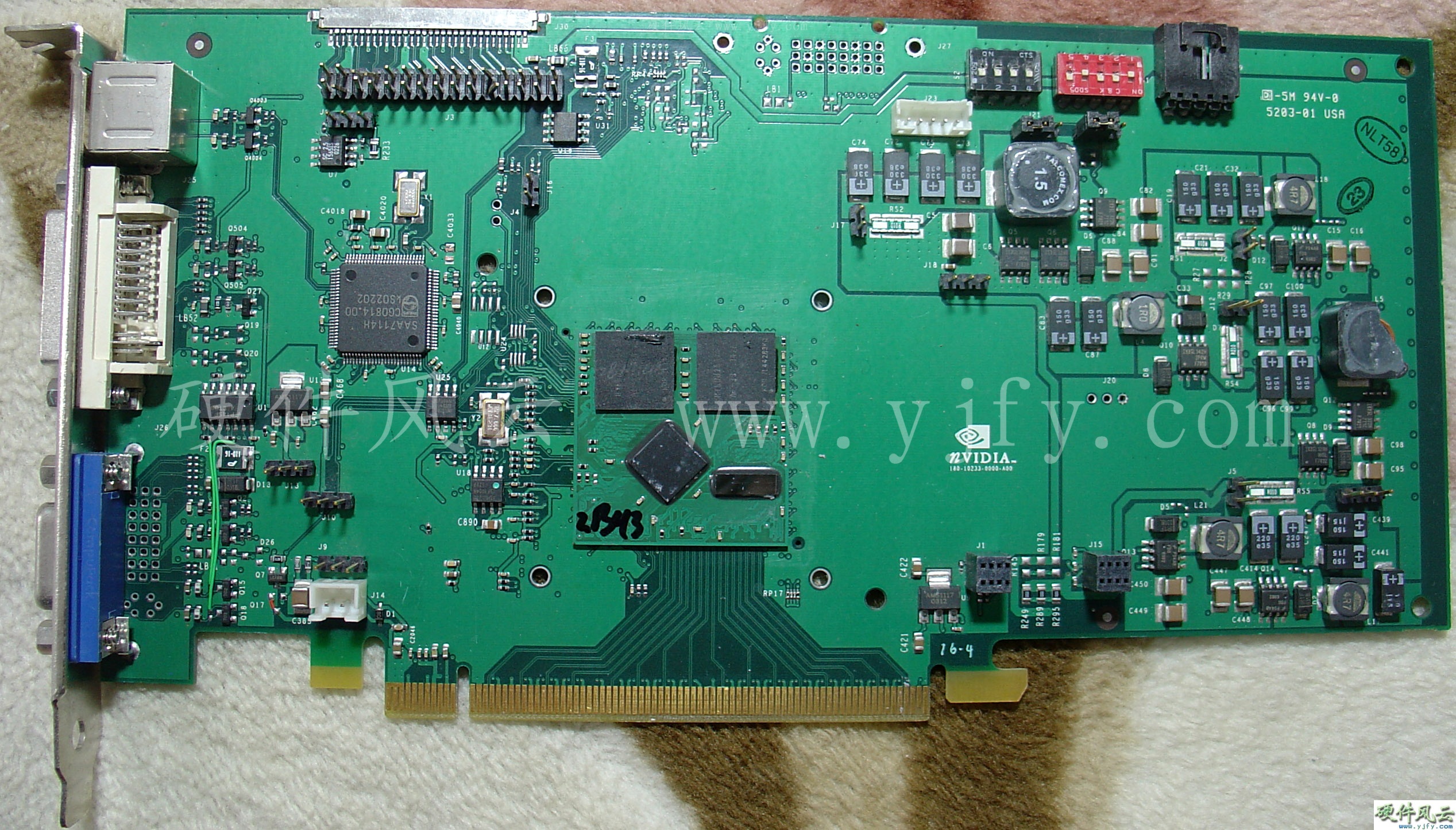
5.4
GeForce FX5700/FX5700 Ultra
2003 �� 10 �� 23 ��������
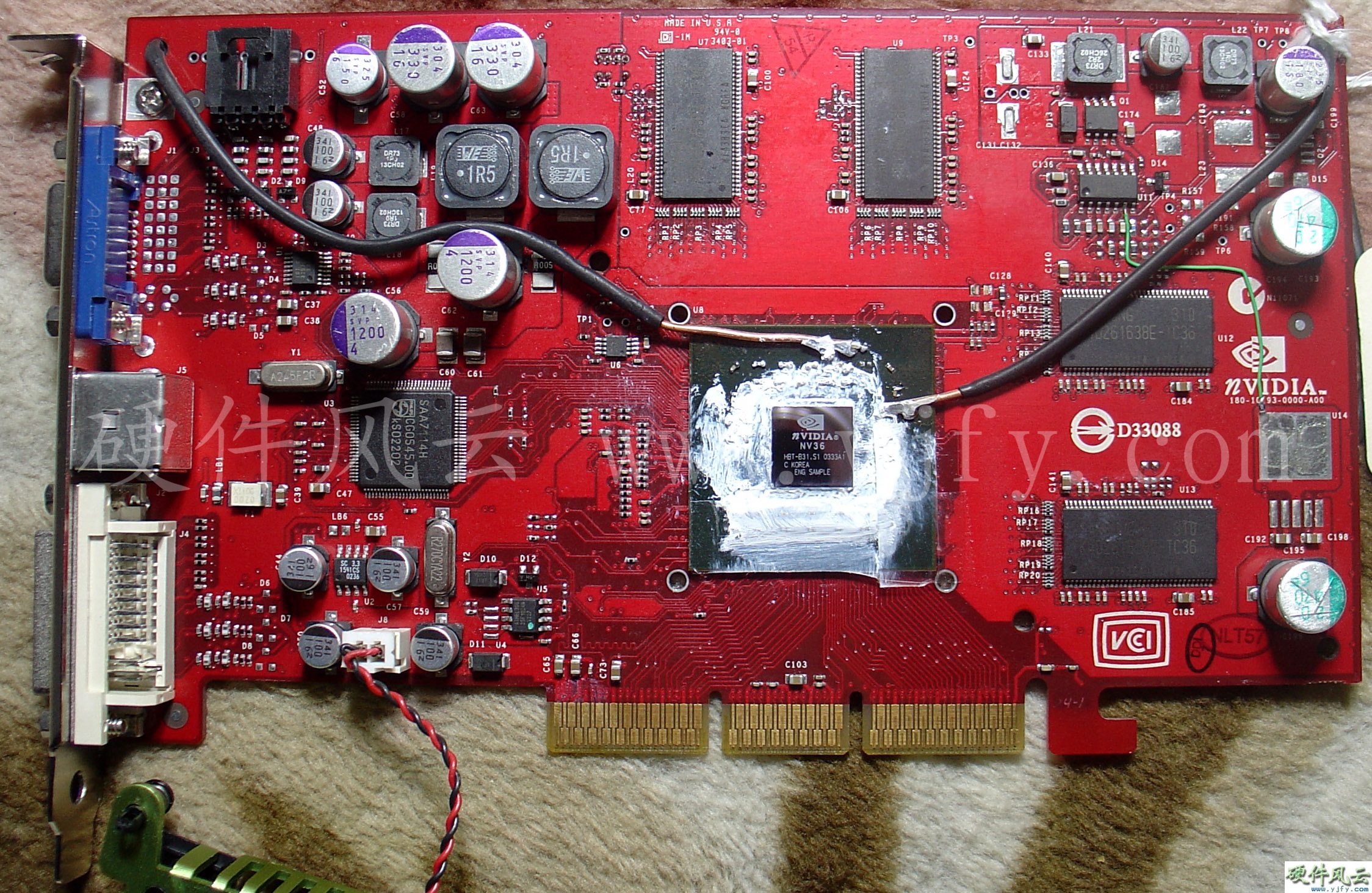
5.4.1 P193
Chip model:NV36 A1 ES
PCB Code:180-10193-0000-A00
оƬ����0333�ܣ�PCB����0334�ܡ�nVIDIA��PCB��ɫ
�Ӷ࣬��ɫ�ķdz��ټ���
GeForce FX5700 Engineering sample

5.4.2 E183
Chip model:NV36S A1
ES
PCB Code:180-10183-0000-A00
оƬ����0334�ܣ�PCB����0330�ܡ�
GeForce FX5700
Engineering sample
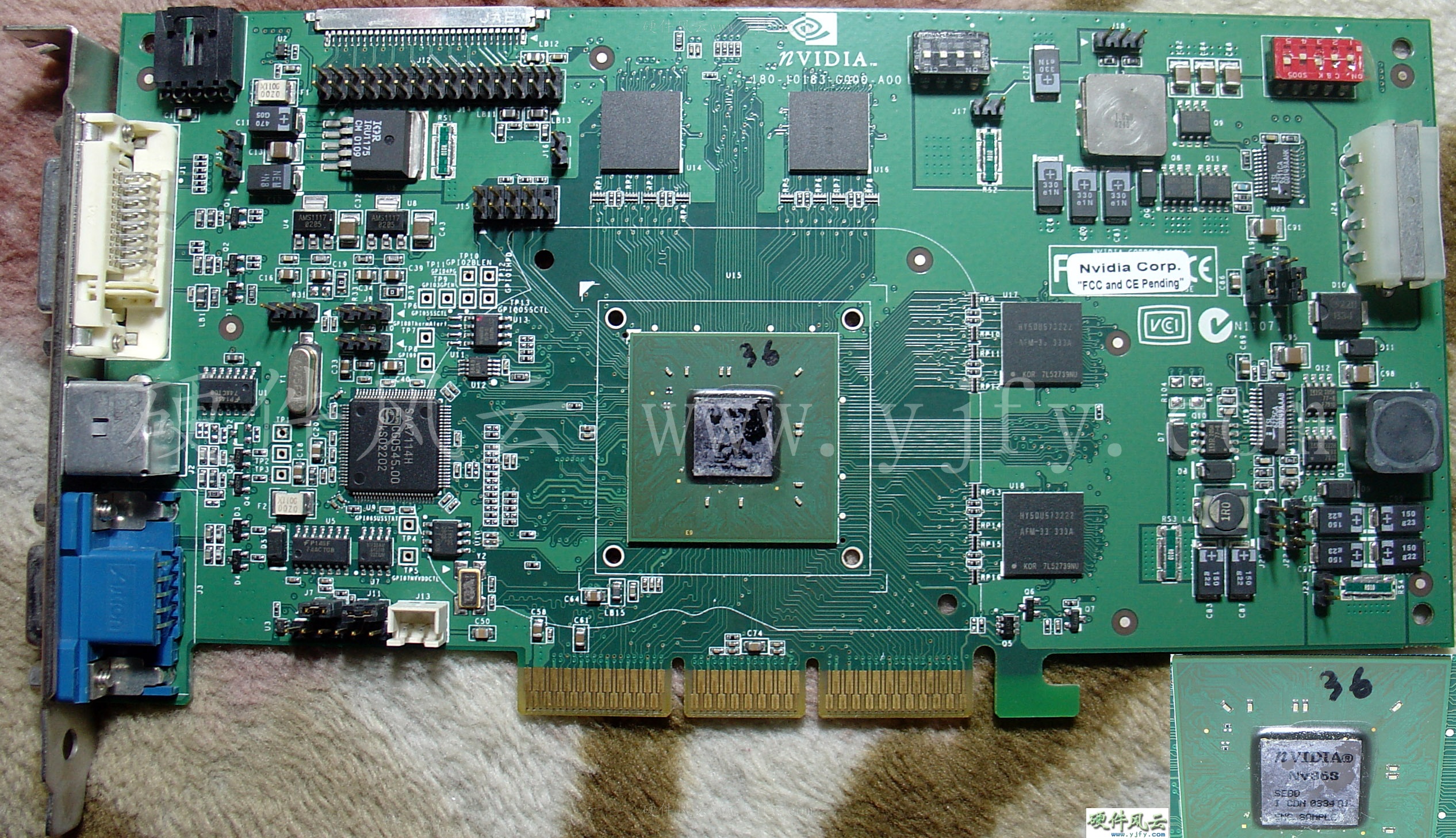
5.4.3 P190
PCB Code:180-10190-0000-A03
Chip model:GF-FX-5700-U-A1
оƬ����0346�ܣ�PCB����0342�ܡ�
GeForce FX5700 Ultra
Engineering sample
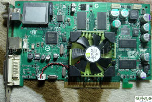
5.5
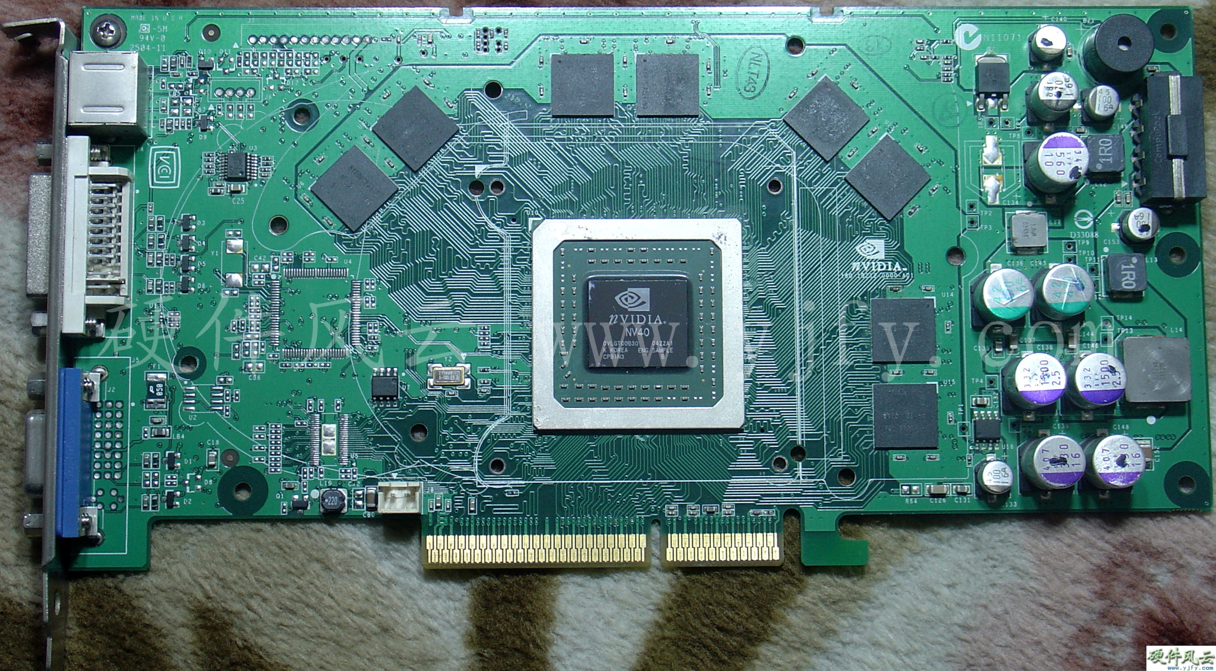
GeForce FX5900/FX5900 Ultra
2003��5��12�շ�����
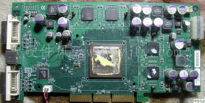
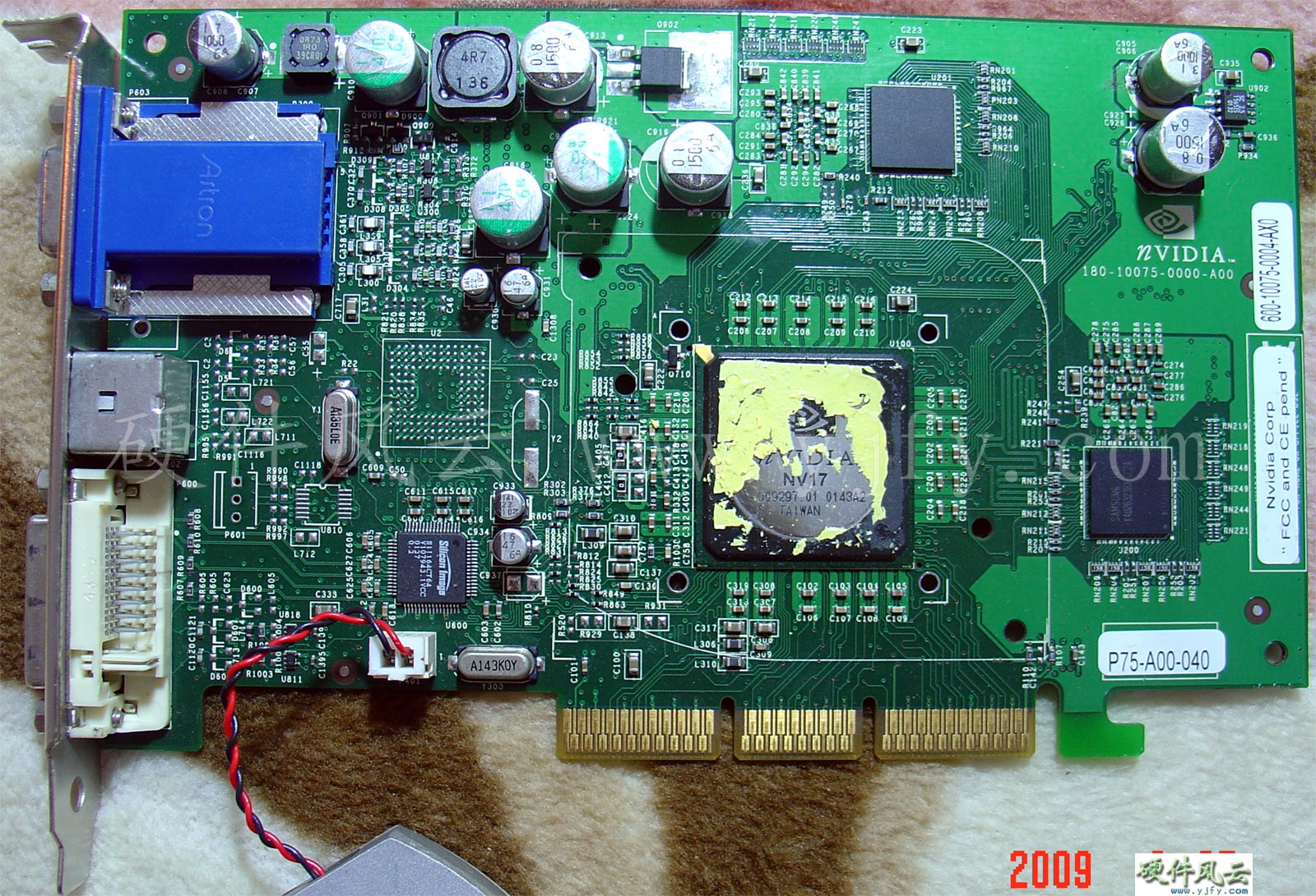
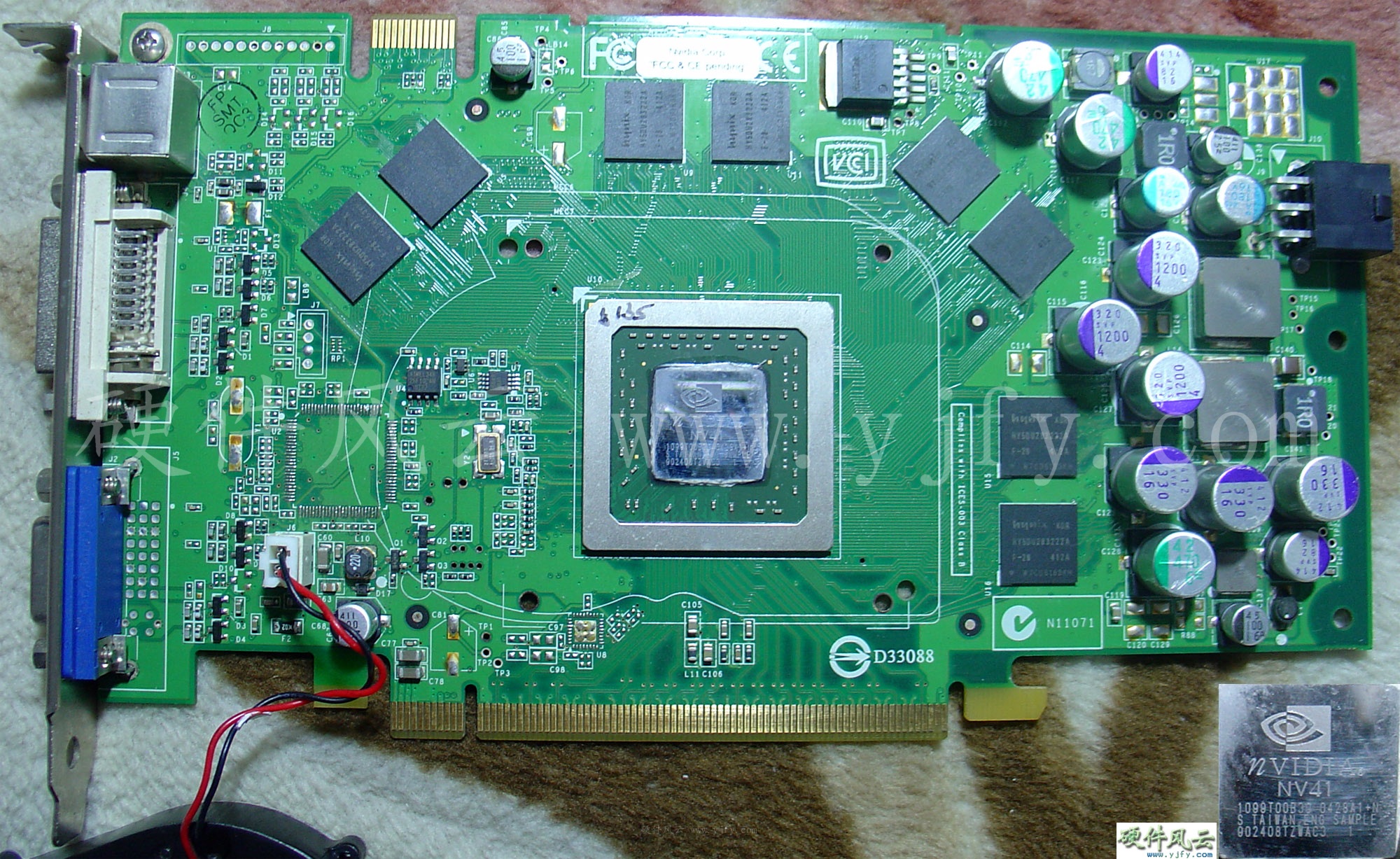
5.5.1 P172-A00
Chip model:NV35 A1
PCB Code:180-10172-0000-A00
оƬ����0310�ܡ�
GeForce FX5900
Engineering sample
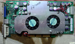
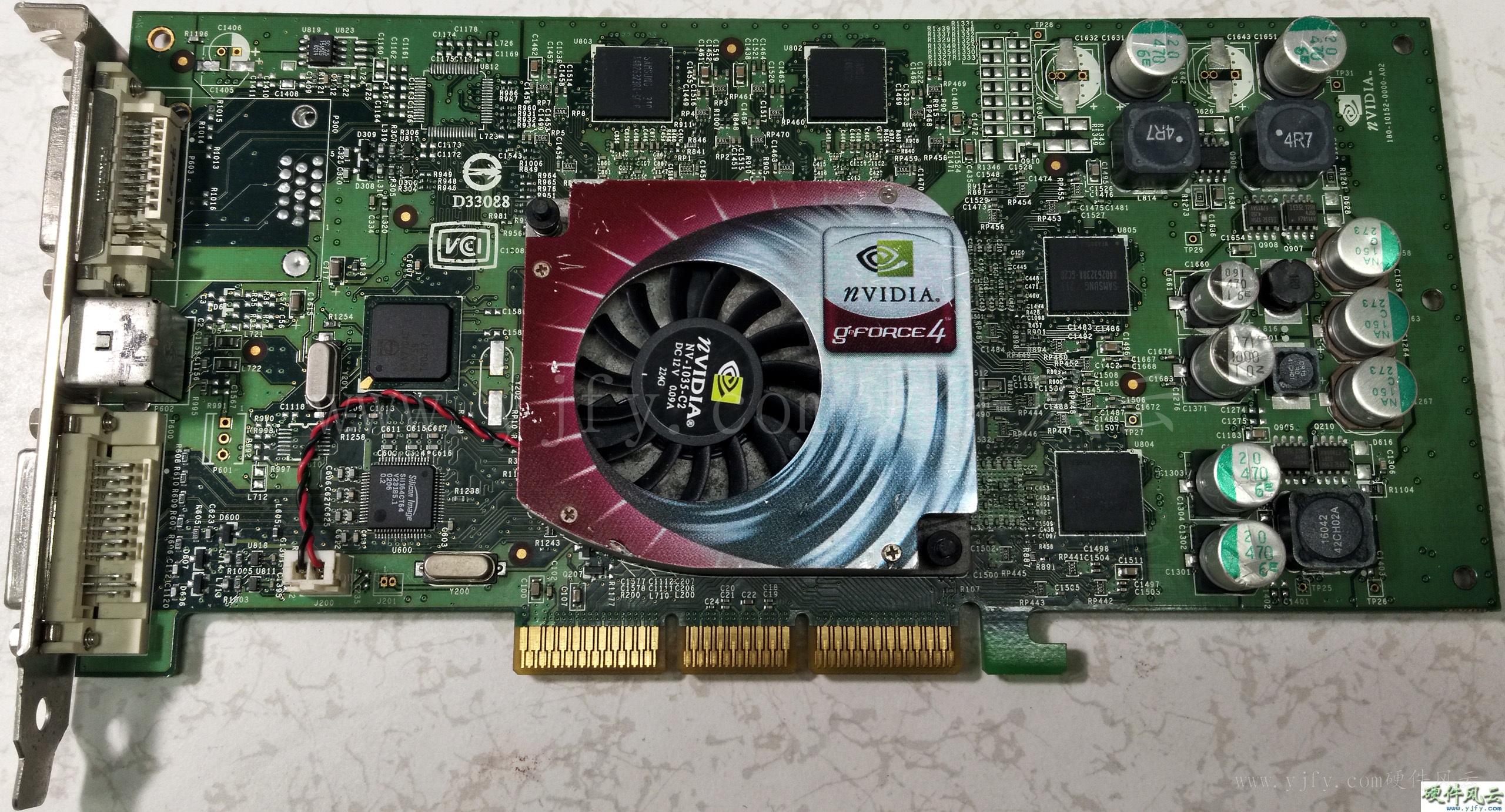
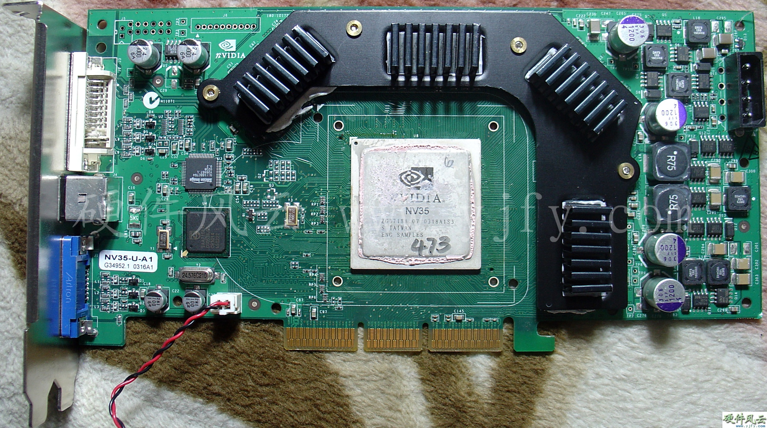
5.5.2 P172-B00
Chip model:NV35-U-A1 ES
PCB Code:180-10172-0000-B00
оƬ����0329�ܣ�PCB����0335�ܡ�
GeForce FX5900 Ultra
Engineering sample

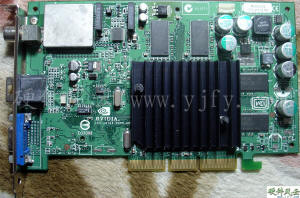
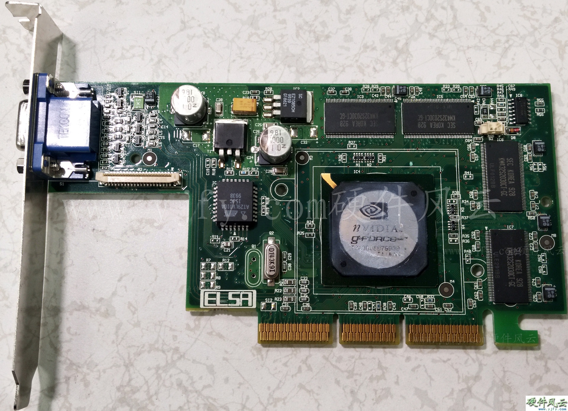
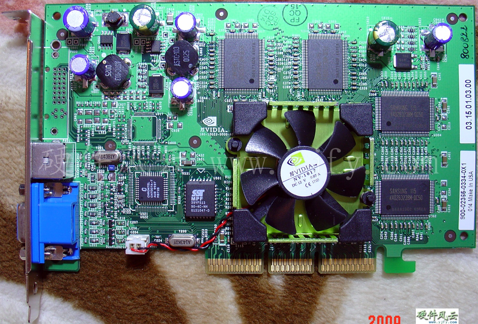
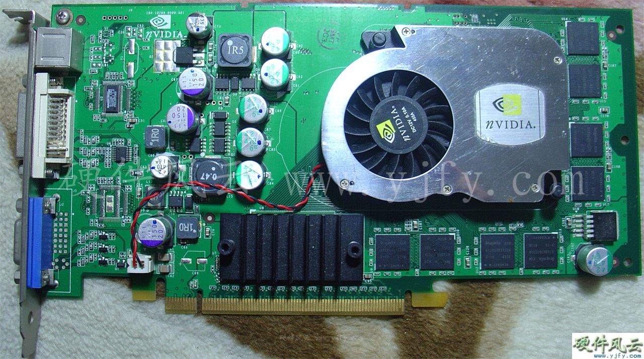
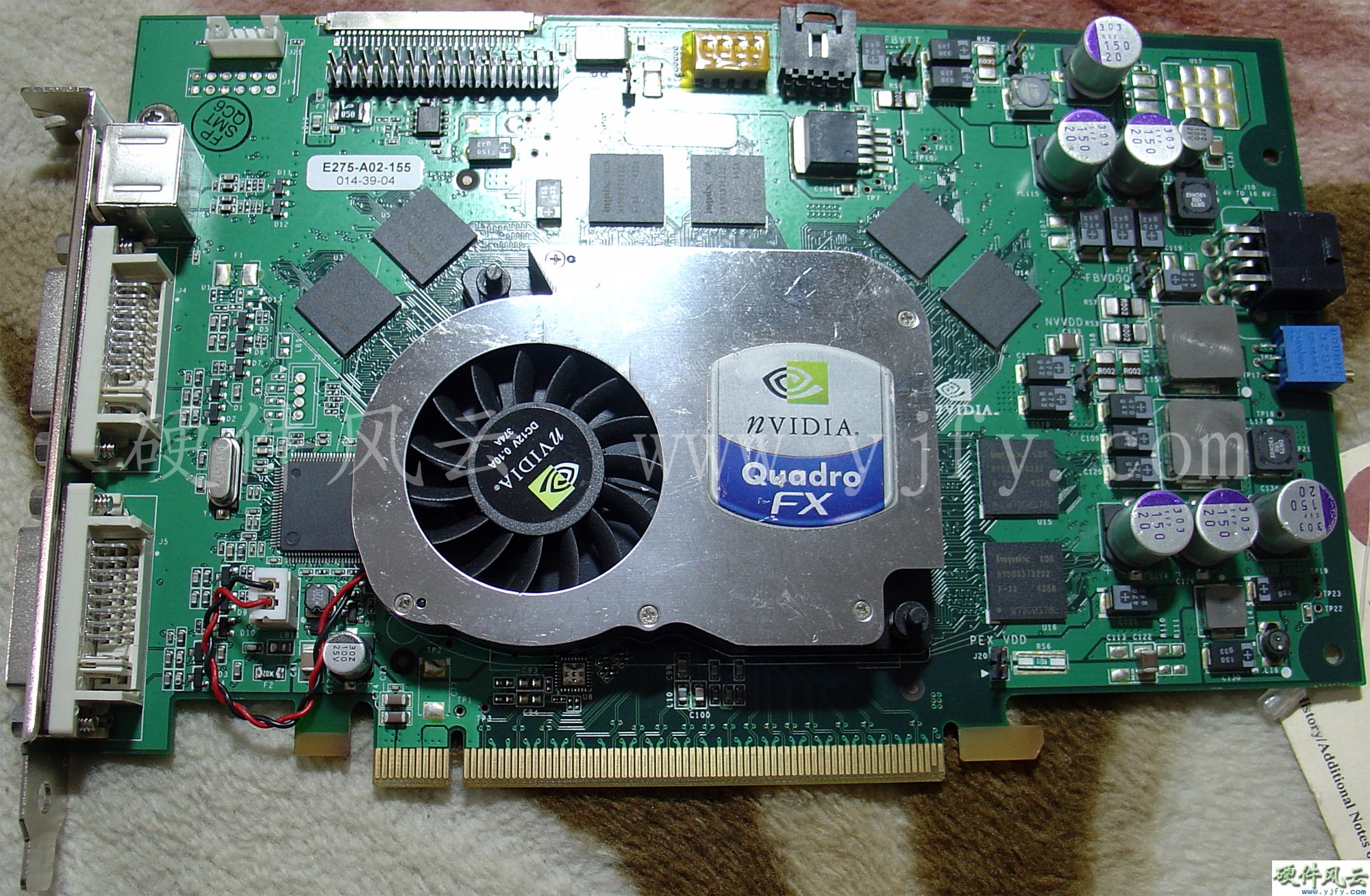
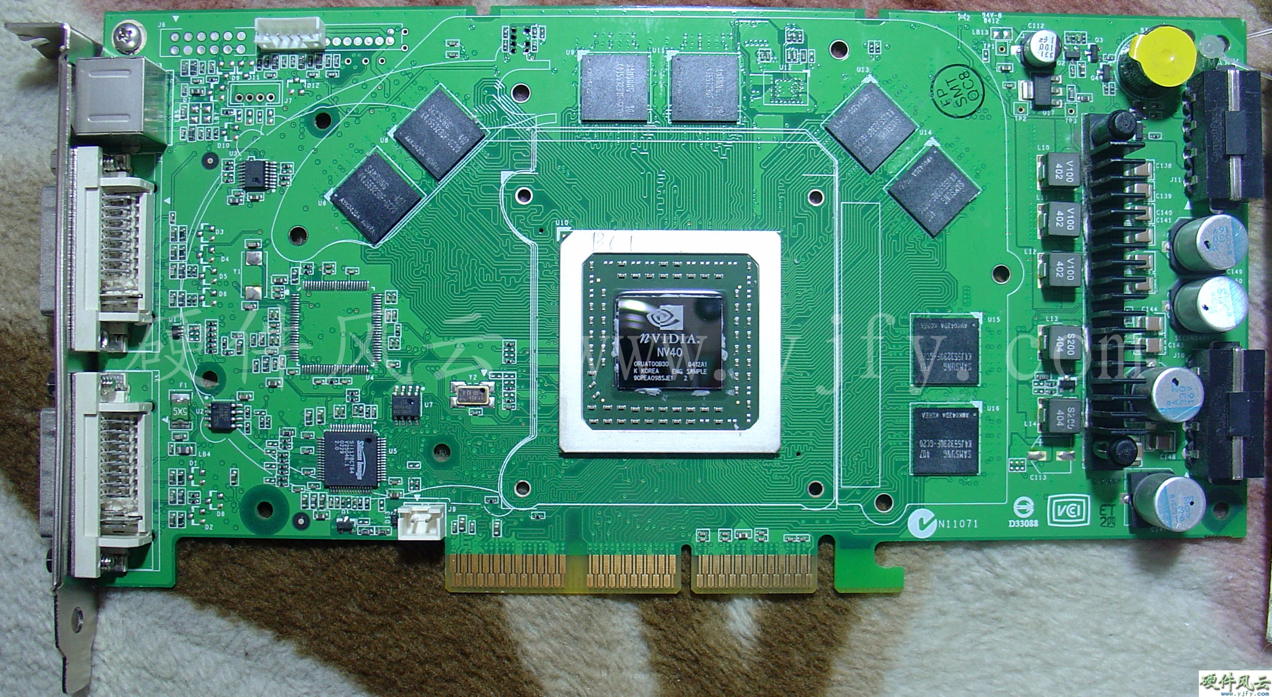
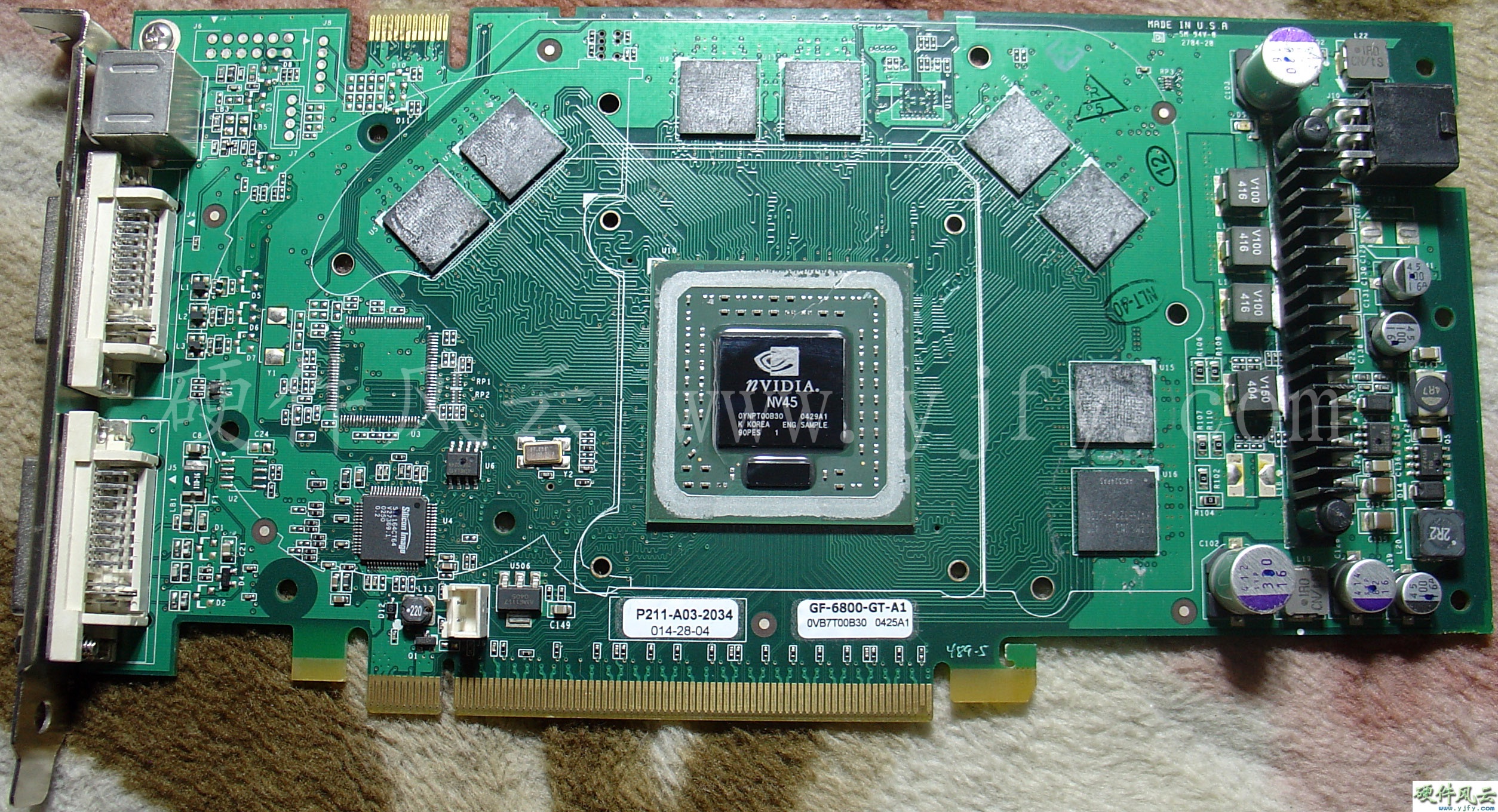
5.6 GeForce FX5950
Ultra
2003��10��23��nVIDIA����GeForce
FX5950 Ultra��
Model:P172-B00
Chip model:FX5900U-A1
PCB Code:180-10172-0000-B00
оƬ����0329�ܣ�PCB����0333�ܡ�
GeForce FX5950 UltraEngineering
sample

5.7 Personal cinema
FX5200
5.7.1 P143
PCB Code:180-10143-0000-B01
Chip model:FX5200 A2
оƬ����0318�ܣ�PCB����0341�ܡ�
Personal cinema
FX5200
Engineering sample
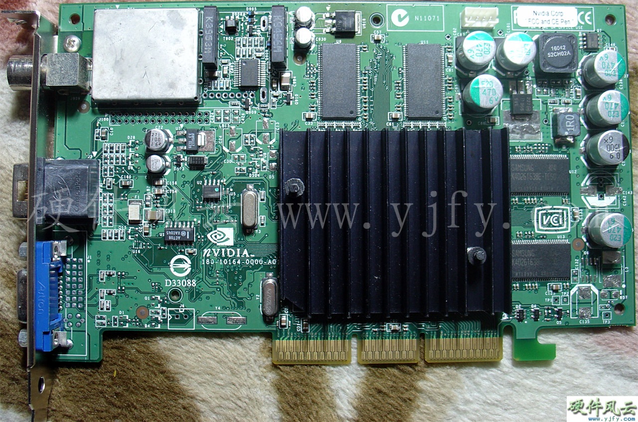
5.7.2 P164
PCB Code:180-10164-0000-A01
Chip model:NV34 A2 ES
оƬ����0308�ܣ�PCB����0306�ܡ�
Personal cinema
FX5200
Engineering sample
5.8 Personal cinema
FX5600
5.8.1 P143 A00
Chip model:NV31 A1+9
ES
PCB Code:180-10143-0000-A00
оƬ����0310�ܣ�PCB����0309�ܡ�
Personal cinema FX5600 Engineering sample
5.8.2 P143 B00
Chip model:FX5600 A1
PCB Code:180-10143-0000-B00
оƬ����0321�ܣ�PCB����0306�ܡ�
Personal cinema FX5600 Engineering sample
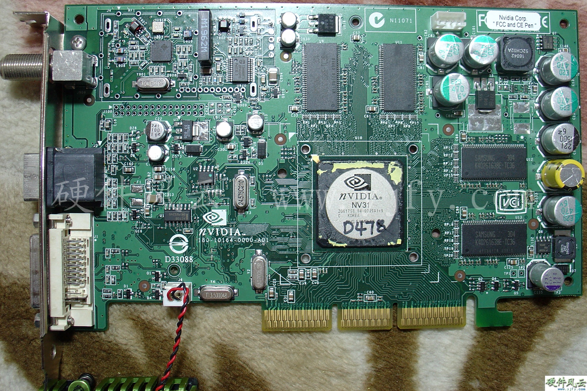
5.8.3 P164
PCB Code:180-10164-0000-A01
Chip model:NV31 A1+9
ES
оƬ����0310�ܣ�PCB����0327�ܡ�
Personal cinema
FX5600
Engineering sample
5.9 Personal cinema
FX5700
Model:P178
PCB Code:180-10178-0000-A02
Chip model:FX5700 A1
оƬ����0403�ܣ�PCB����0404�ܡ�
Personal cinema
FX5700
Engineering sample

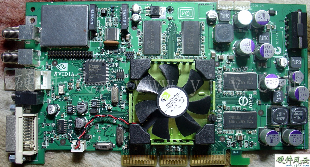
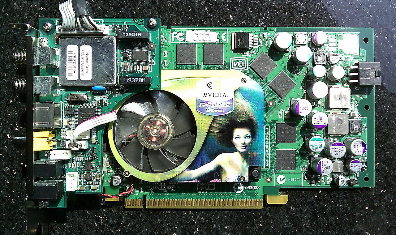
����Personal
cinema FX5900�Ǵ�����Ƶ�ӿ���GeForce FX5900�Կ���
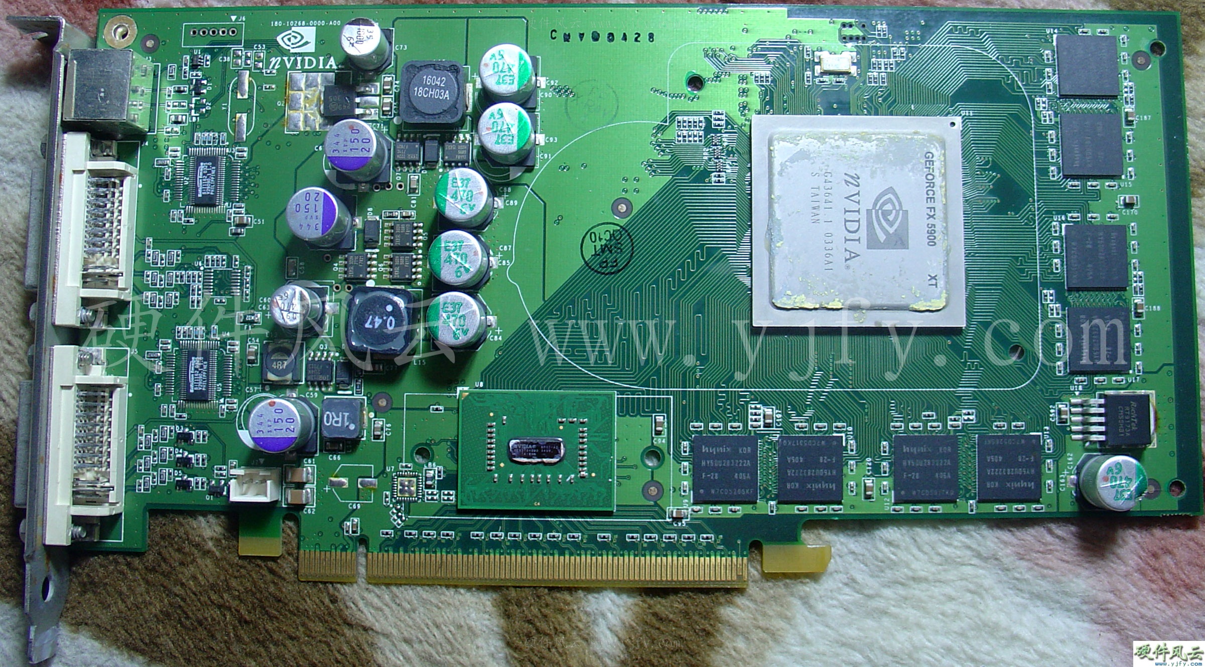
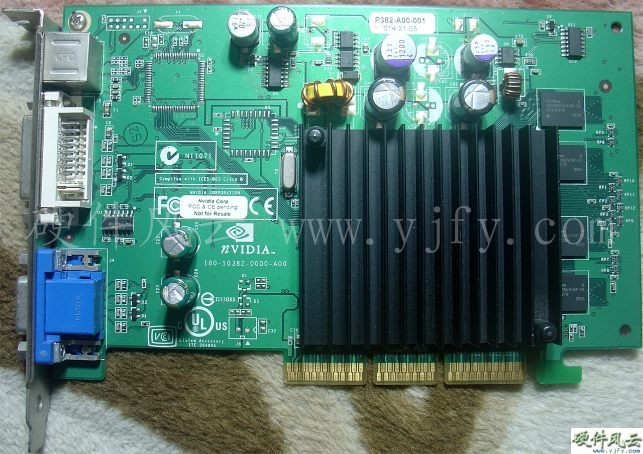
5.10 GeForce PCX5900
2004��2��17��nVIDIA
����GeForce PCX ϵ���Կ���GeForce PCX5950��NV35����GeForce
PCX5750��NV36����GeForce PCX5300��NV34����GeForce
PCX4300��GeForce4 MX 4000��,���DZ������Ǵ��� AGP-to-PCI
Express �Ž�оƬBR02�� AGP ����
5.10.1 P268 A00
Chip model:5900XT
PCB Code:180-10268-0000-A00
оƬ����0336�ܣ�PCB����0409�ܡ�
GeForce PCX5900 Engineering sample
5.10.2 P268 A01
Chip model:5900XT
PCB Code:180-10268-0000-A01
оƬ����0349�ܣ�PCB����0421�ܡ�
GeForce PCX5900
Engineering sample

nVIDIA������GeForce
PCX5950����ΪGeforce PCX5900�������г���ʹ�ô˰����������ν��GeForce
PCX5950�Կ���
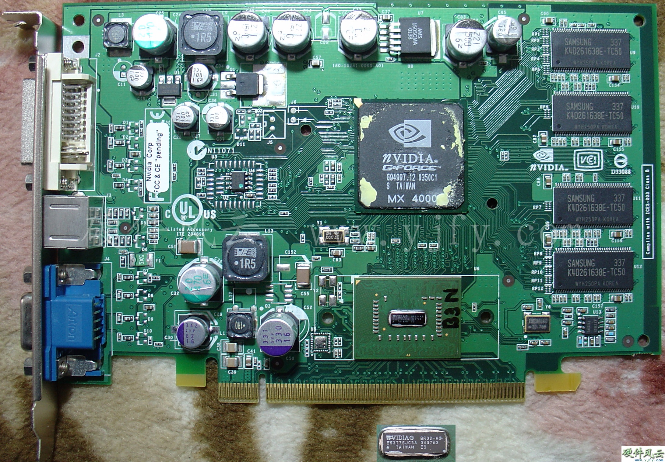
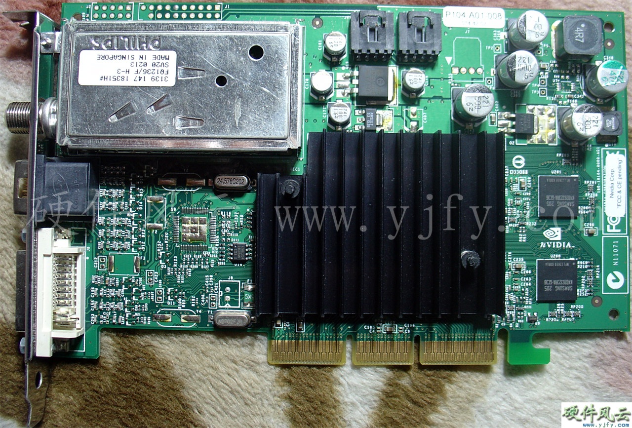
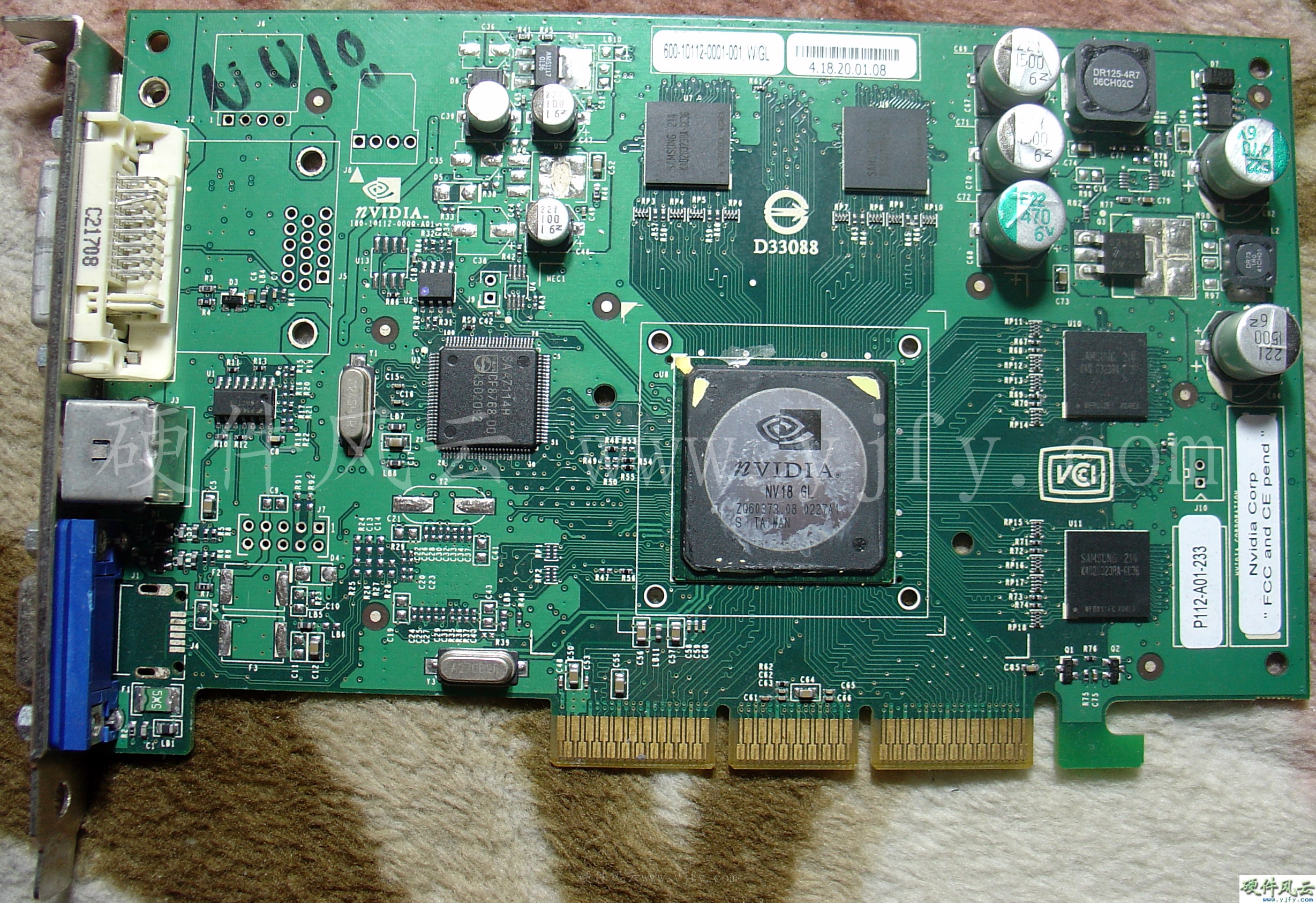
5.11 GeForce PCX5300
5.11.1 E286
Chip model:GF-FX-5200-B1
PCB Code:180-10286-0000-B00
оƬ����0404�ܣ�PCB����0407�ܡ�
GeForce PCX5300 Engineering sample

5.11.2 P241
Chip model:FX5200
B1S1 ES
PCB Code:180-10241-0000-A01
��ʾоƬ����0344�ܣ�PCB����0352�ܡ�BR02-A2
ESоƬ����0407�ܡ�
GeForce PCX5300 Engineering sample

GeForce PCX 5750��NV36����P269���ͣ���P241���Ƶ���ۡ�
5.12 GeForce PCX5300
MCM
�����ƶ��豸��MXM�ӿ��Կ���
5.12.1 P233
PCB Code:180-10233-0000-B01
Chip model:NV37 A1 ES
оƬ����0405�ܣ�PCB����0405�ܡ�
GeForce PCX5300 MCM Engineering sample
MCM��Multi-Chip
Module����оƬģ�飬��һ���㾧��die����оƬ�����ɵ�·�İ�װ����װ������Package�������ַ�װ��������һ�������Ϸ�װ�������������ϵ��㾧��ͨ����ʾоƬ�ڽ���װһ����ʾ�����㾧��ǰ���ᵽ��nVIDIA
GeForce4
Go����2/4���Դ����ʾ���ķ�װ��һ�������ϣ���ʡ�ռ估�����ܺģ��������ƶ�оƬ�ϡ�����PCI-Eʱ����nVIDIA��BR02�Ž�оƬ��ͨ��MCM��װ��BR02оƬ����ʾоƬ�Լ��Դ��װ��ͬһ�����ϡ�
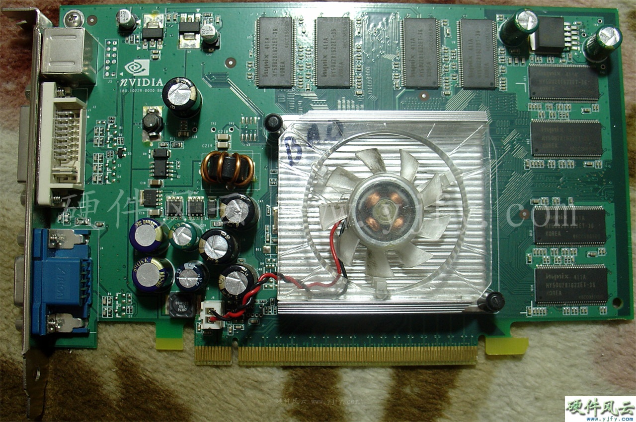
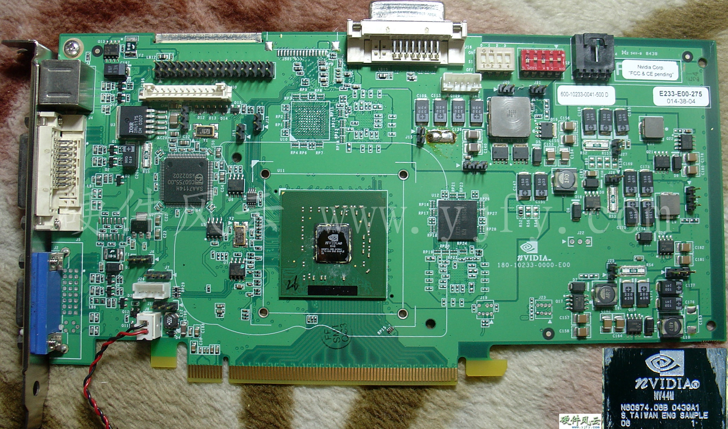
5.12.2 E233
PCB Code:180-10233-0000-A00
PCB����0352�ܡ�BR02оƬ����ʾоƬ�Լ��Դ��װ��ͬһ�����ϡ�
GeForce PCX5300 MCM Engineering sample

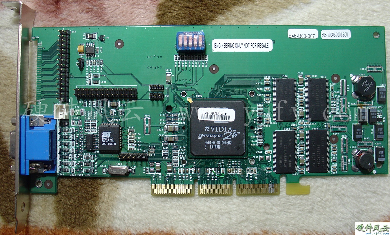
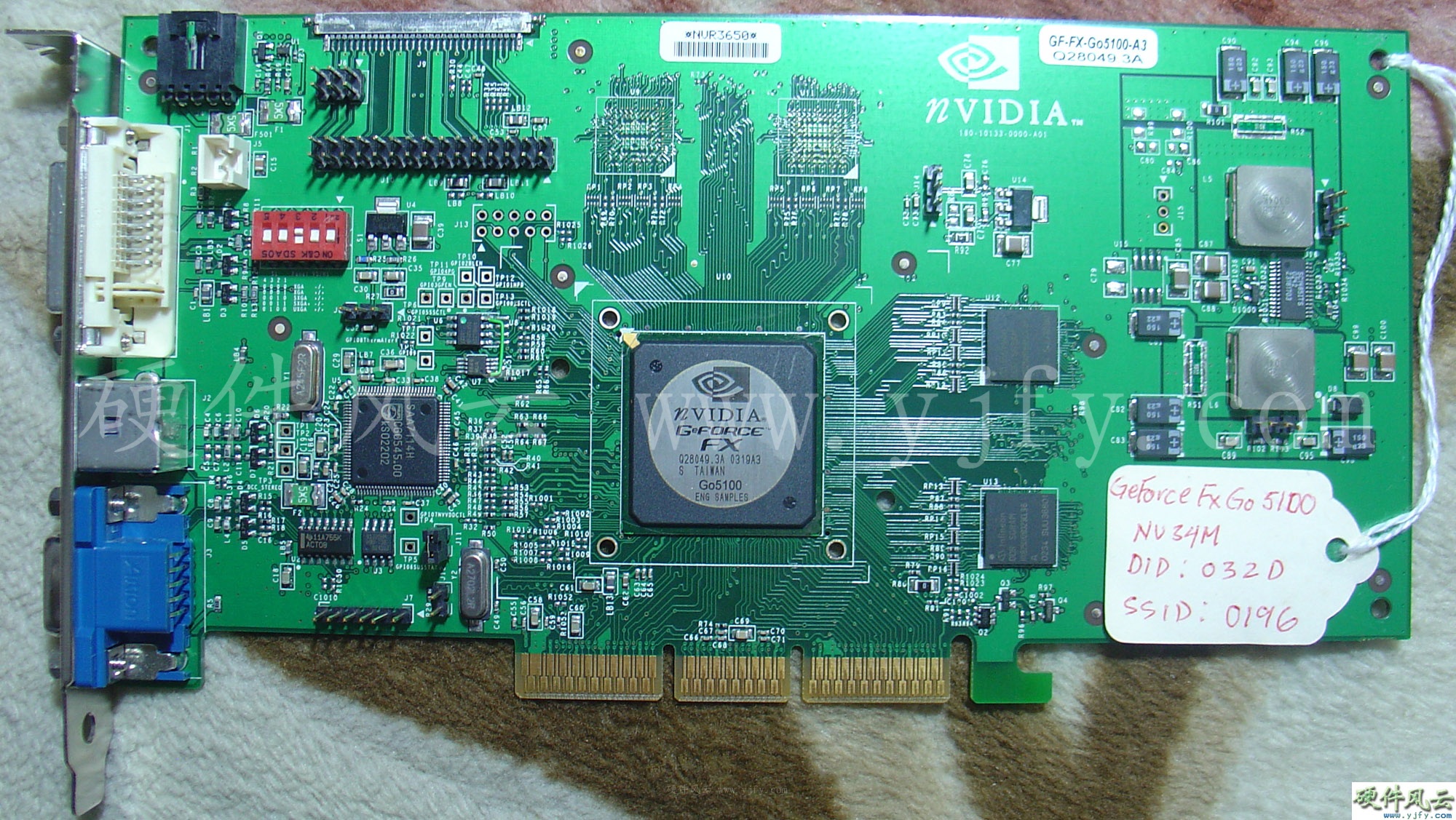
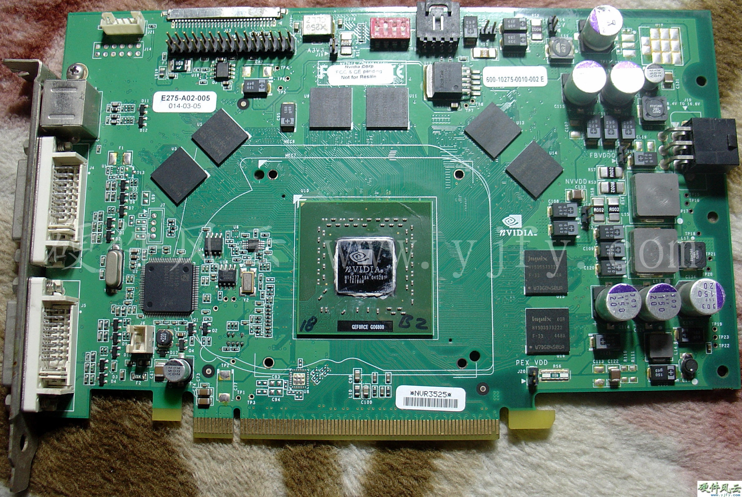
5.13 GeForce FX
Go5100
Model:E133
Chip model:Go5100
A3 ES
PCB Code:180-10133-0000-A01
�ƶ��档оƬ����0319�ܣ�PCB����0317�ܡ�
GeForce FX Go5100 Engineering sample
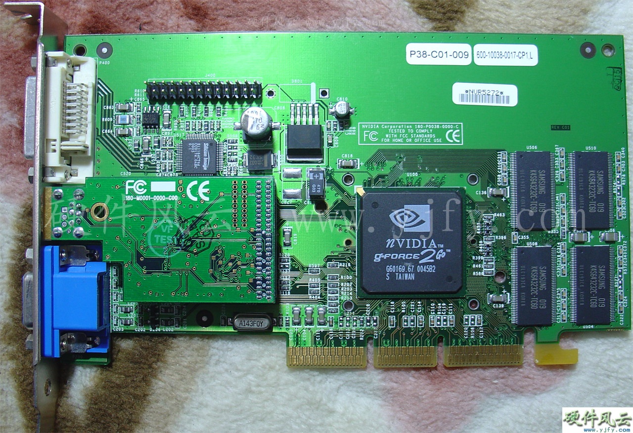
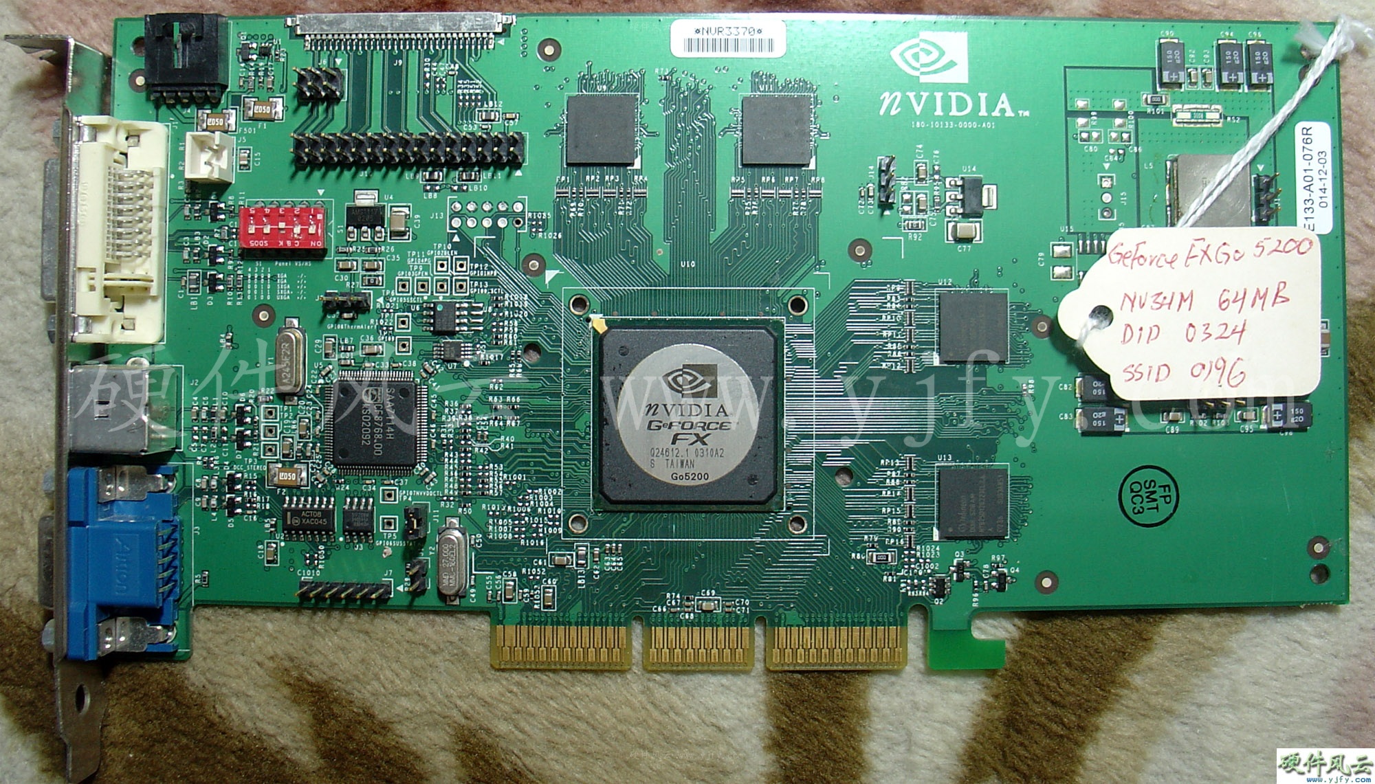
5.14 GeForce FX
Go5200
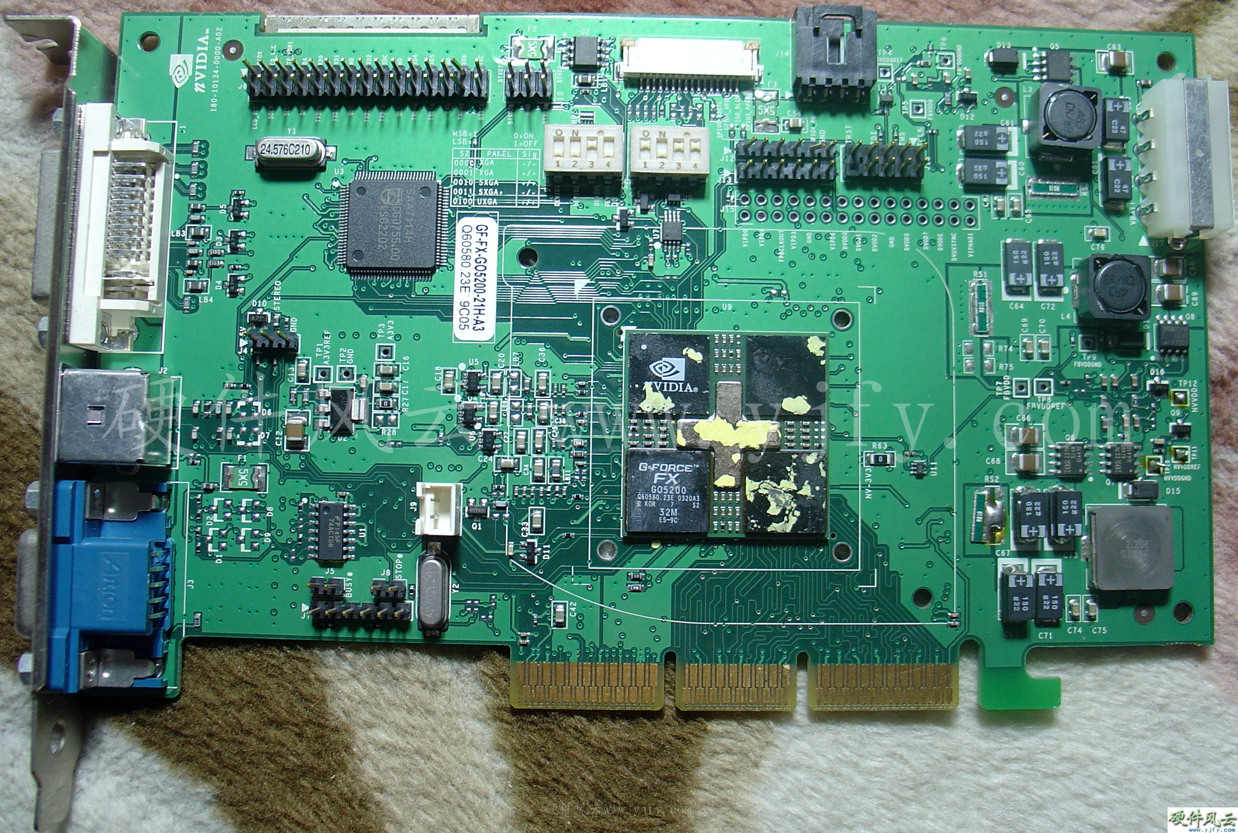
5.14.1 E133
Chip model:Go5200 A2
PCB Code:180-10133-0000-A01
�ƶ��档оƬ����0310�ܣ�PCB����0305�ܡ�
GeForce FX Go5200 Engineering sample
5.14.2 E134
Chip model:Go5200 A3
ES 64M
PCB Code:180-10134-0000-A02
�ƶ��档оƬ����0320�ܣ�PCB����0319�ܡ�
GeForce FX Go5200
MCM
Engineering sample
5.14.3 E15
PCB Code:180-10015-0000-A00
Chip model:MVP34 A2
ES 64MB
�ƶ��档оƬ����0309�ܣ�PCB����0317�ܡ�
GeForce FX Go5200
MCM
Engineering sample
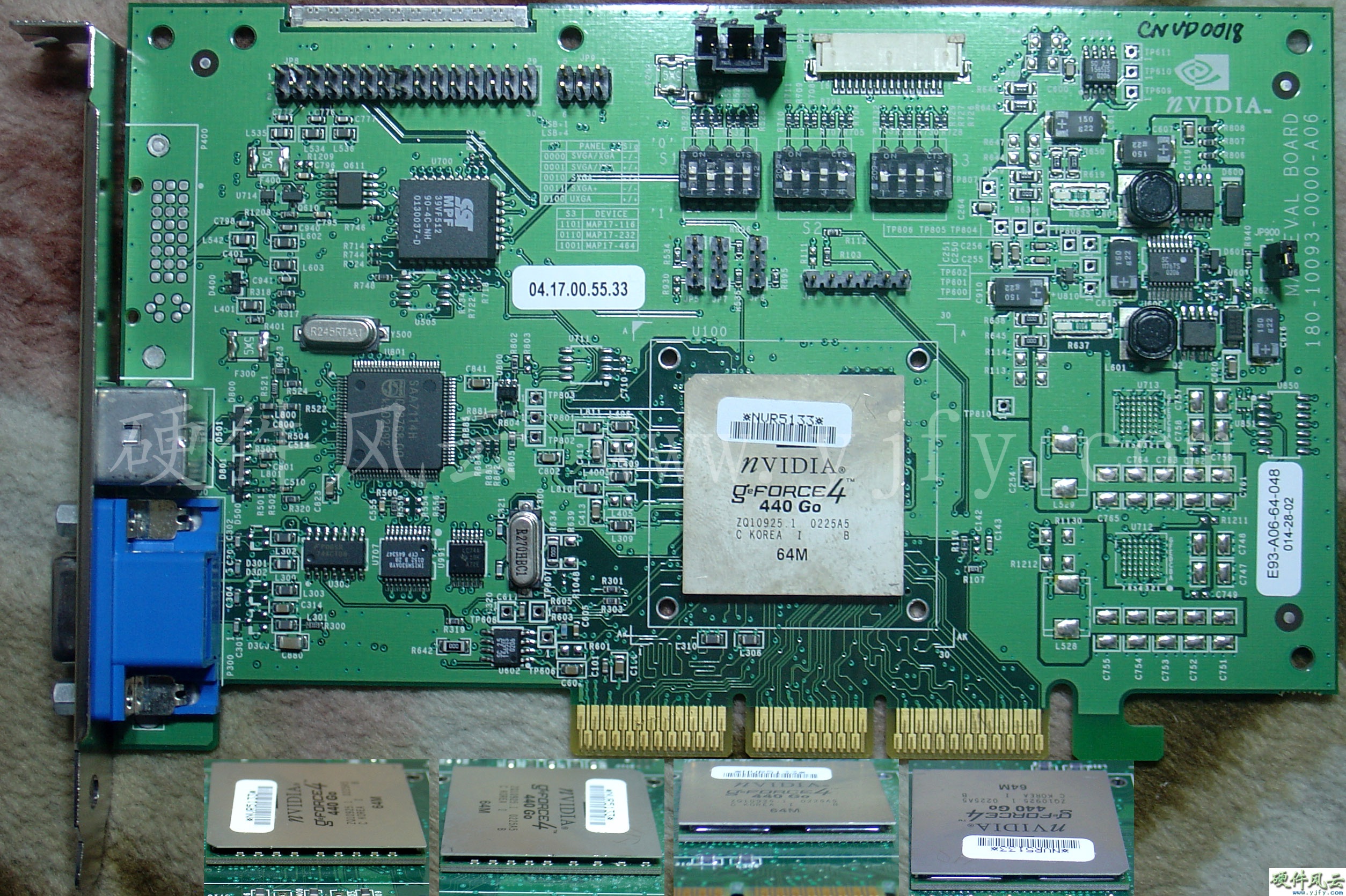
5.15 GeForce FX
Go5250
Model:E133
Chip model:Go5250 A3
PCB Code:180-10133-0000-A01
�ƶ��档оƬ����0327�ܣ�PCB����0329�ܡ�
GeForce FX Go5250 Engineering sample
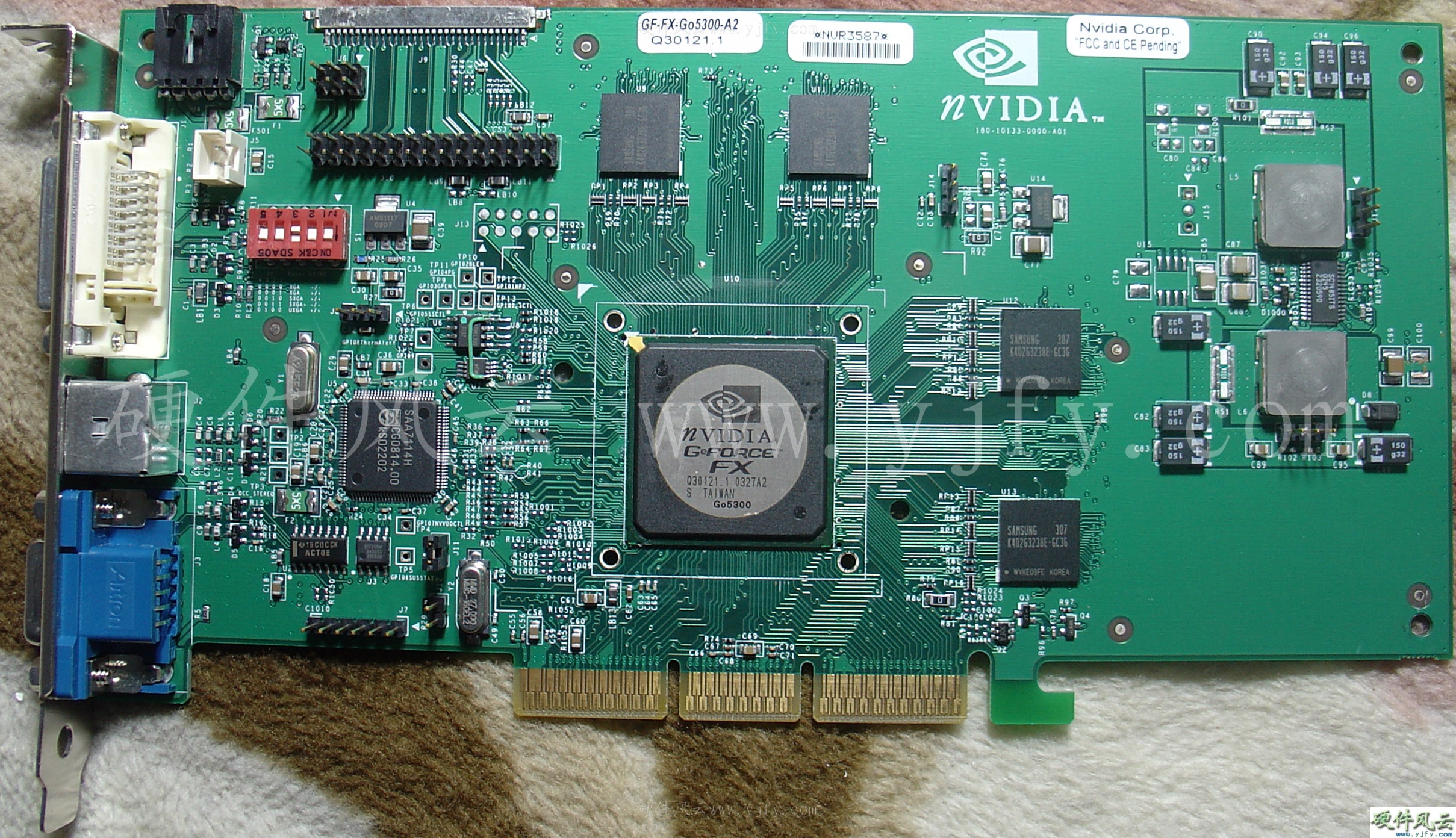
5.16 GeForce FX
Go5300
Model:E133
Chip model:Go5300 A2
PCB Code:180-10133-0000-A01
�ƶ��档оƬ����0327�ܣ�PCB����0329�ܡ�
GeForce FX Go5300 Engineering sample
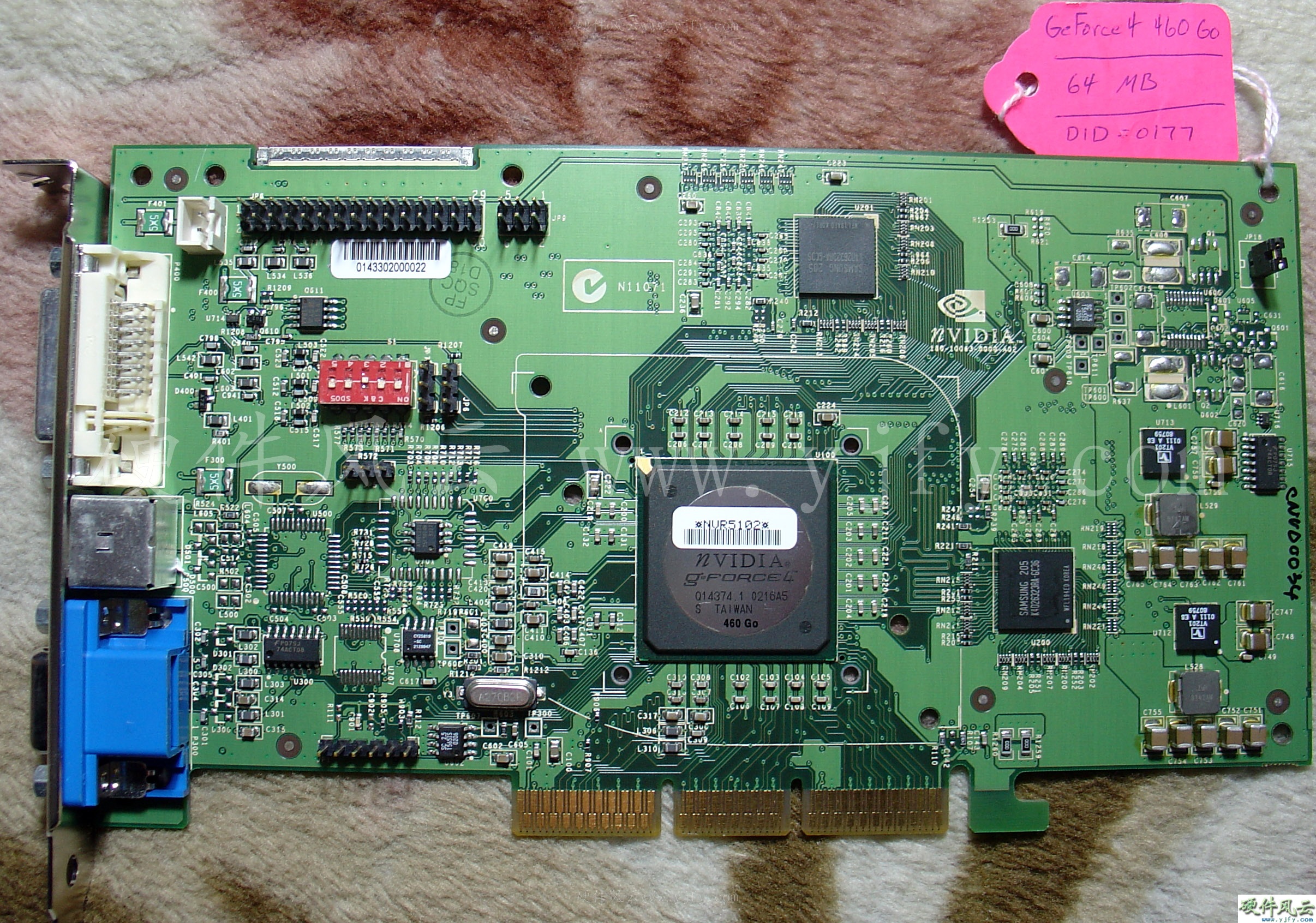
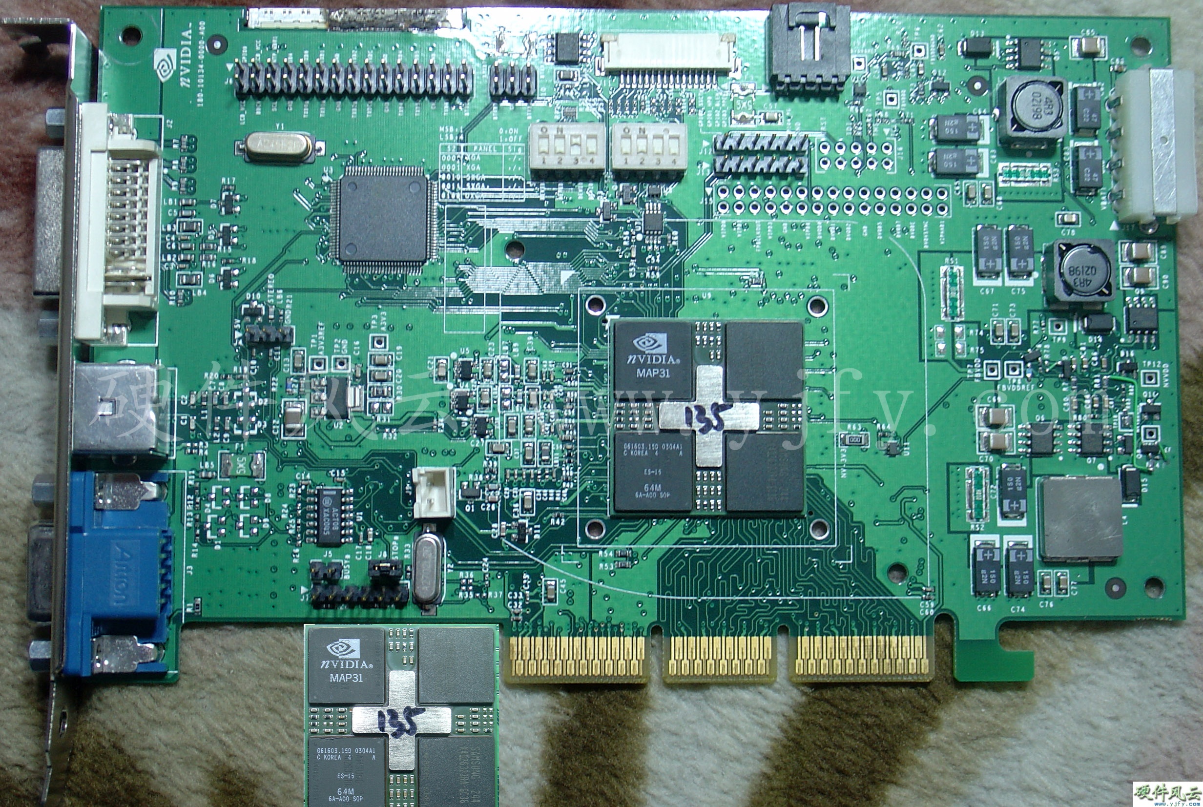
5.17 GeForce FX
Go5600
5.17.1 E133
PCB Code:180-10133-0000-A01
Chip model:Go5600 A1
�ƶ��档оƬ����0338�ܣ�PCB����0308�ܡ�
GeForce FX Go5600 Engineering sample
GeForce FX Go5600
MCM
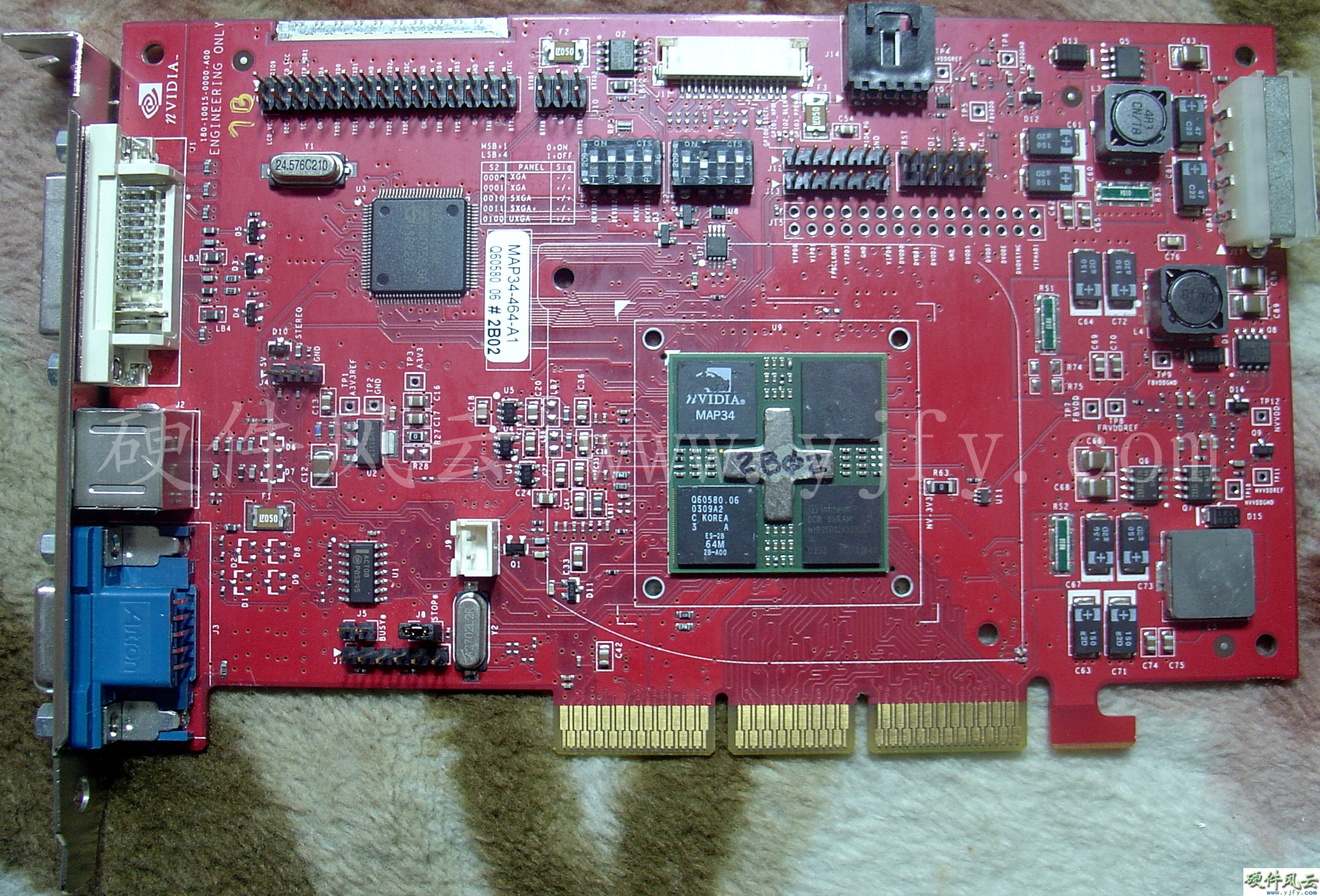
5.17.2 E134
PCB Code:180-10134-0000-A00
Chip model:MAP31
A1 ES
�ƶ��档оƬ����0304�ܣ�PCB����0251�ܡ�
GeForce FX Go5600 MCM Engineering sample
5.18 GeForce FX
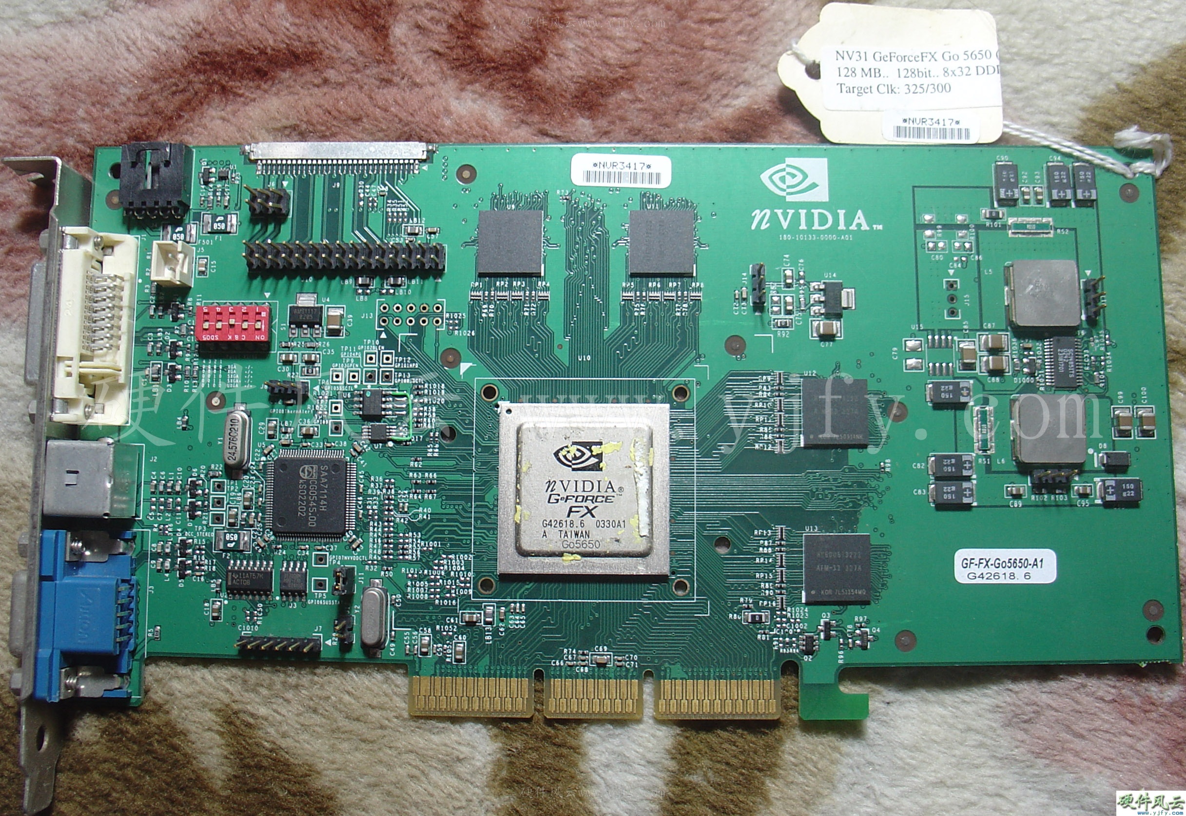
Go5650
Model:E133
Chip model:Go5650 A1
PCB Code:180-10133-0000-A01
�ƶ��档оƬ����0330�ܣ�PCB����0315�ܡ�
GeForce FX Go5650
Engineering sample
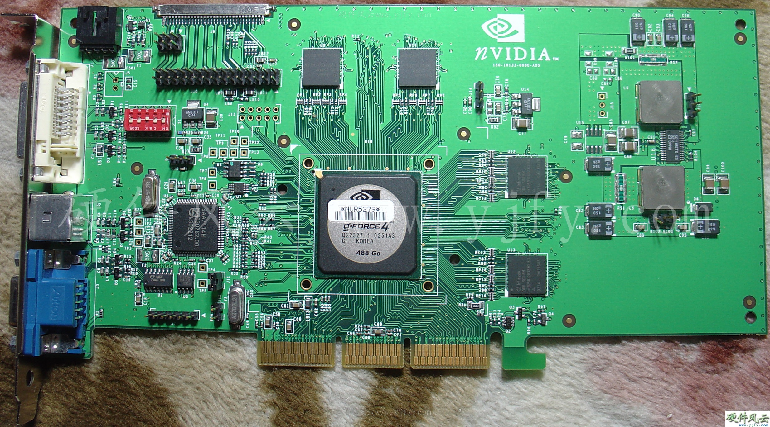
5.19 GeForce FX
Go5700
5.19.1 E183
Chip model:NV36M
A1 ES
PCB Code:180-10183-0000-A01
�ƶ��档оƬ����0344�ܣ�PCB����0344�ܡ�
GeForce FX Go5700
Engineering sample
5.19.2 P183
Chip model:GF-FX-Go5700
A1
PCB Code:180-10183-0000-A01
�ƶ��档оƬ����0346�ܣ�PCB����0350�ܡ�
GeForce FX Go5700
Engineering sample
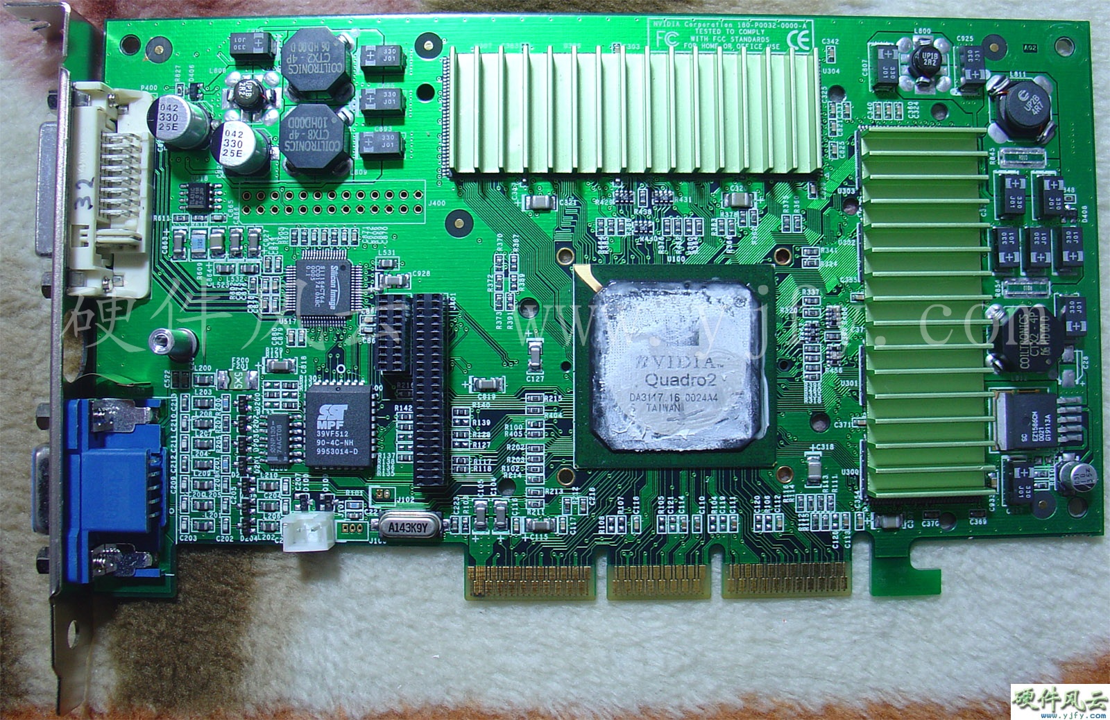
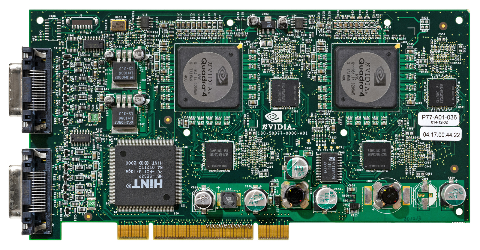
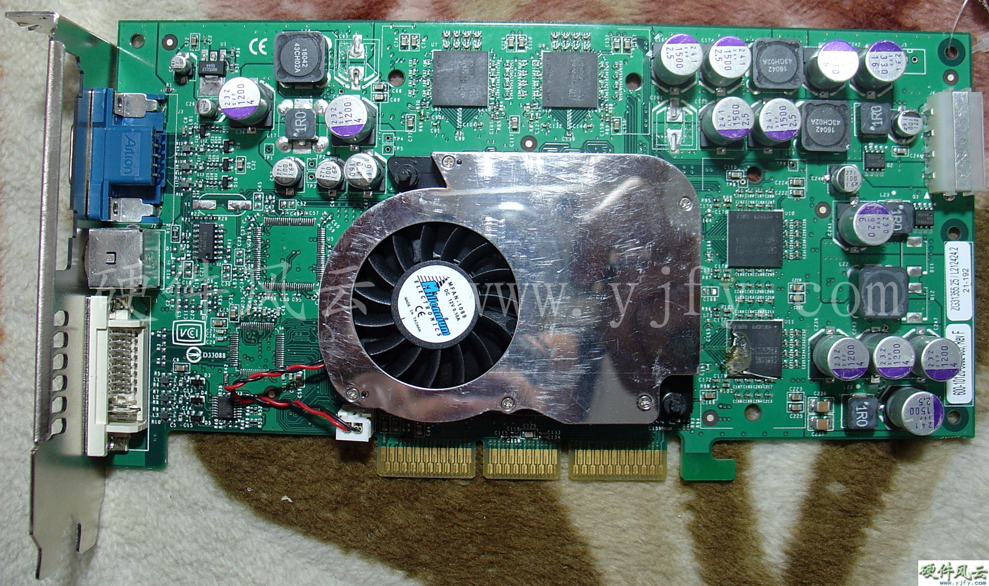
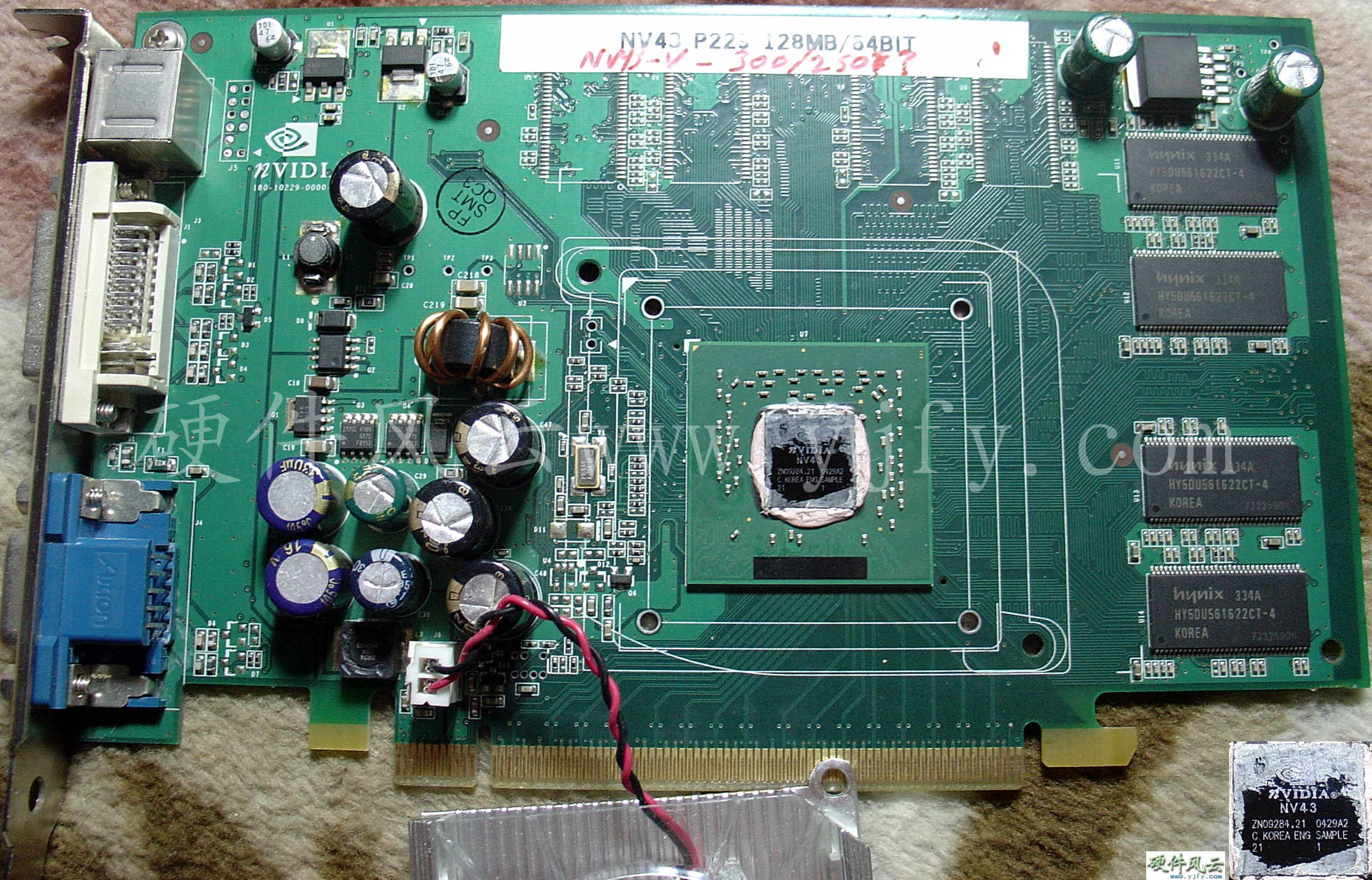
5.20 Quadro FX1000
Model:P126
PCB Code:180-10126-0000-A04
Chip model:NV30GL A1
2003��1��21�շ�����оƬ����0244�ܣ�PCB����0249�ܡ�
Quadro FX1000
Engineering sample
������Quadro
FX1000����Quadro FX2000��P128���͡�
5.21 Quadro FX2000
Model:P128
PCB Code:180-10128-0000-A00
Chip model:FX2000-A2X-ES
2003��1��21�շ�����оƬ����0252�ܣ�PCB����0301�ܡ�
Quadro FX2000
Engineering sample
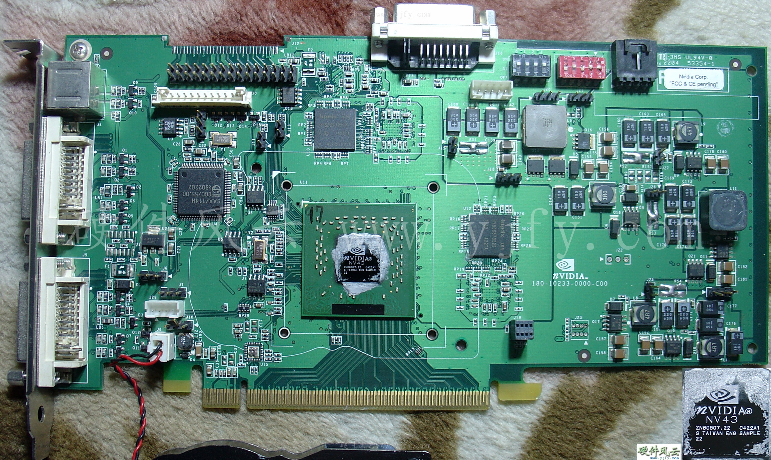
5.22 Quadro FX3000
2003��7��22�շ�����
5.22.1 P170-B01
Chip model:NV35GL
A1S2 ES
PCB Code:180-10170-0000-B01
оƬ����0314�ܣ�PCB����0314�ܡ�
Quadro FX3000 Engineering sample
5.22.2 E174-A00
PCB Code:180-10174-0000-A00
Chip model:FX3000 A1
оƬ����0319�ܣ�PCB����0321�ܡ�
Quadro FX3000 Engineering sample
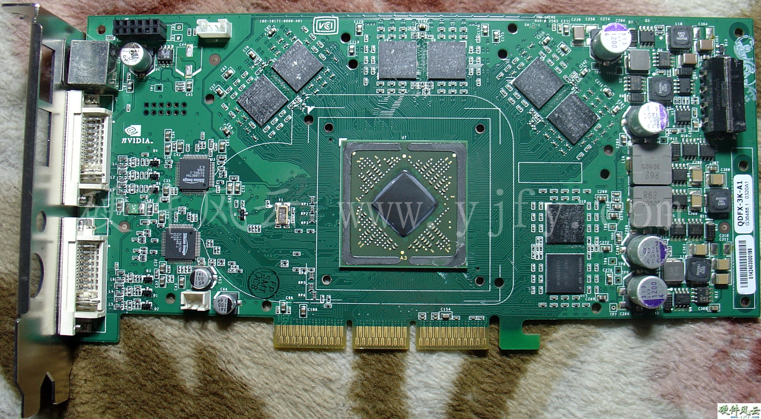
5.22.3 P171-B00
PCB Code:180-10171-0000-B00
Chip model:FX3000 A1
оƬ����0333�ܣ�PCB����0334�ܡ�
Quadro FX3000 Engineering sample
5.22.4 P171-A01
Chip model:Quadro
FX3000 A1
PCB Code:180-10171-0000-A01
оƬ����0320�ܣ�PCB����0325�ܡ�
Quadro FX3000 Engineering sample

�˰���Quadro
FX3000�Կ�����P154�ӿ�(֧����Ƶ����ͬ����֡����ͬ������)����Quadro
FX3000G��
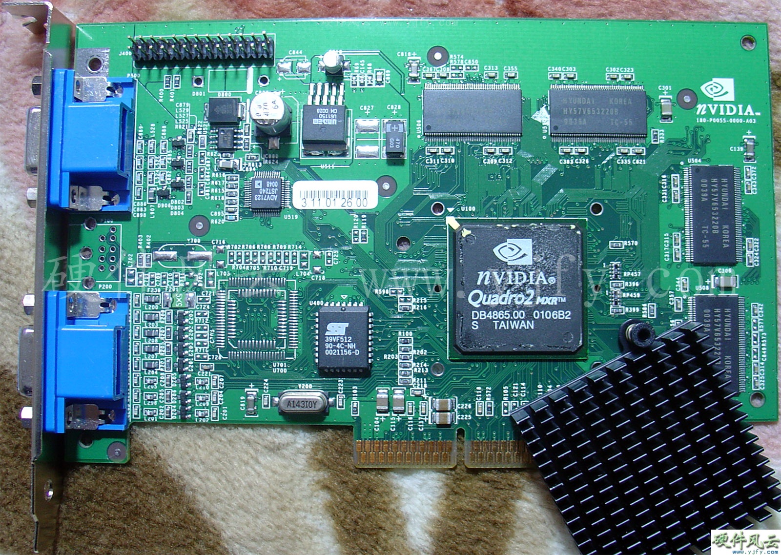
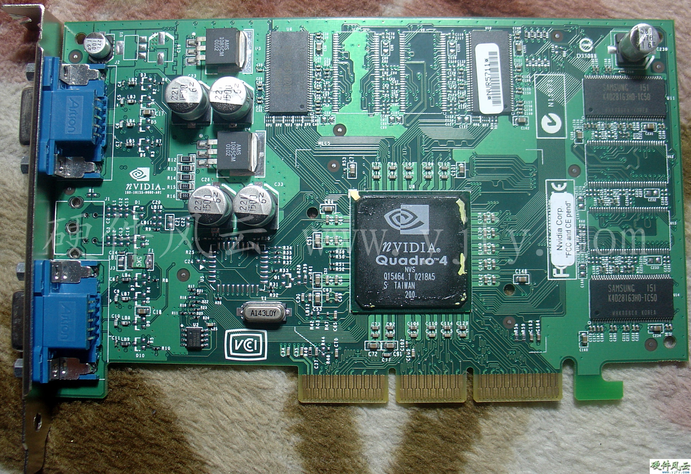
5.23 Quadro FX500
2003��5��21�շ�����
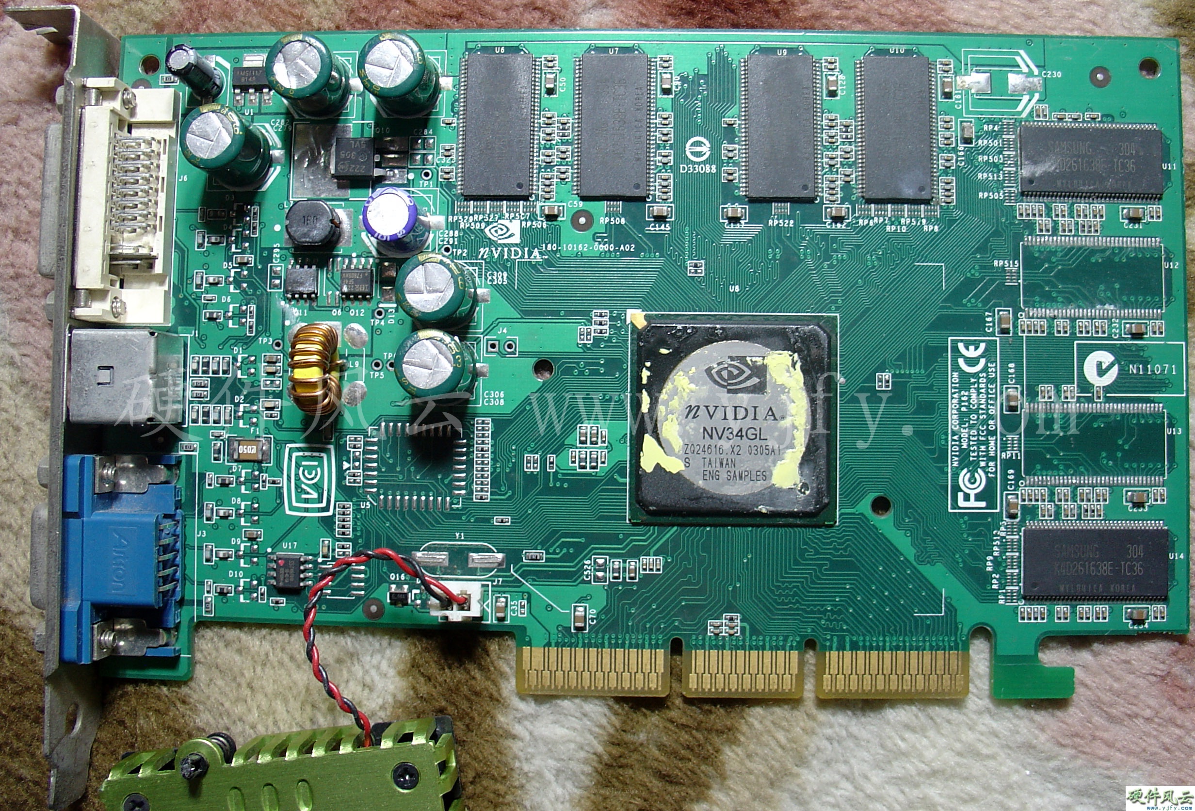
5.23.1 P162
Chip model:NV34GL A1
ES
PCB Code:180-10162-0000-A02
оƬ����0305�ܣ�PCB����0307�ܡ�
Quadro FX500 Engineering sample
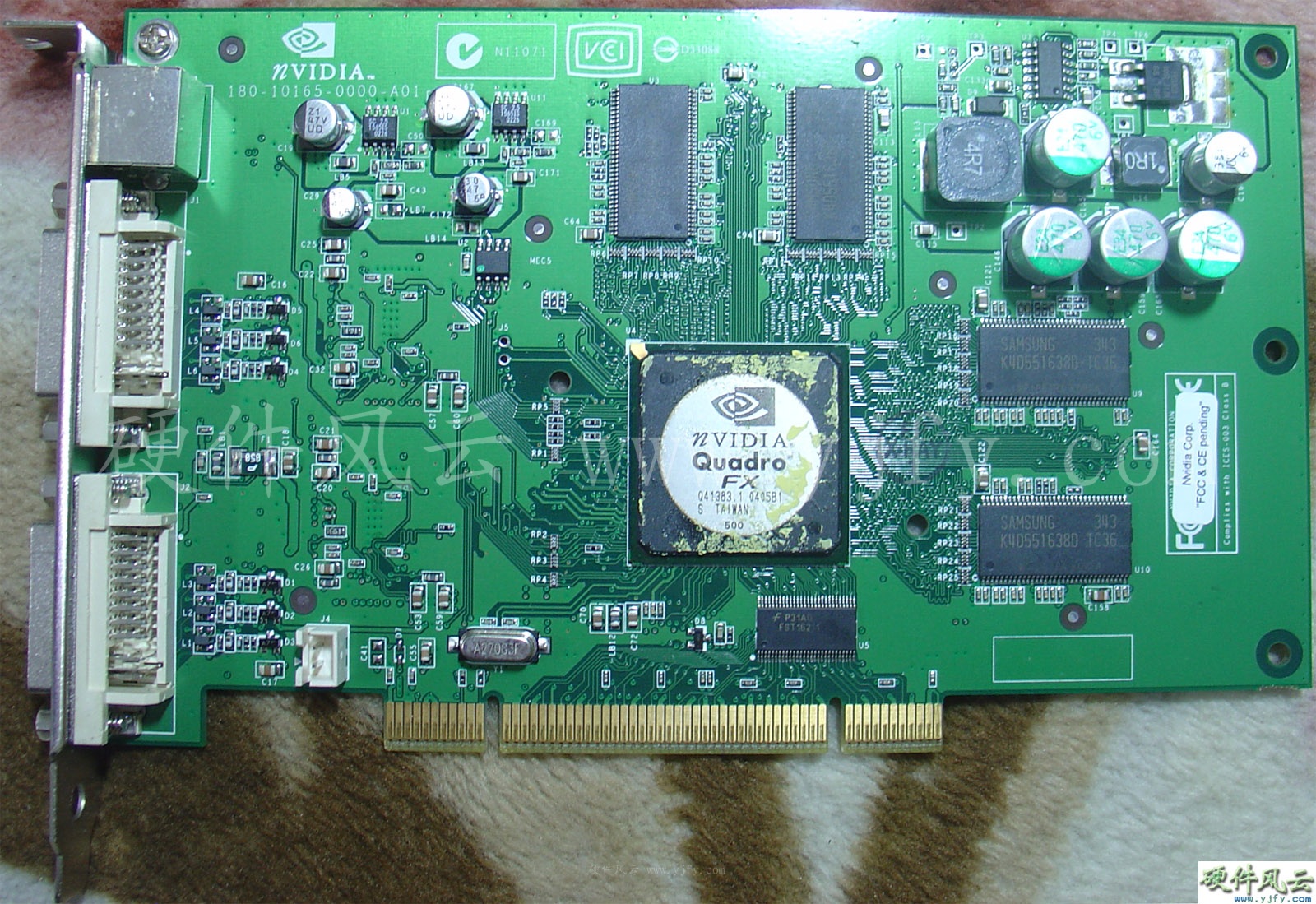
5.23.2 P165
Chip model:QUADRO FX
500 B1
PCB Code:180-10165-0000-A01
оƬ����0405�ܣ�PCB����0407�ܡ�
Quadro FX500 Engineering sample

5.24 Quadro FX700
2004��3��17�շ�����
5.24.1 E133
PCB Code:180-10133-0000-A00
Chip model:NV31GL_A1+
оƬ����0302�ܣ�PCB����0252�ܡ�
Quadro FX700 Engineering sample

5.24.2 P141
Chip model:NV31GL A1+
PCB Code:
û����PCB
Code��ԭ�Ϳ��dz��ټ���������180-10141-0000-A01��
оƬ����0302�ܣ�PCB����0250�ܡ�
Quadro FX700 Engineering sample
����Quadro
FX1100��NV36GL��ʹ��P192���͡�Quadro FX1300��NV36GL��ʹ��P268(GeForce PCX
5900/5950)���ͣ��Լ�nVIDIA NVS 280��NV34���ȡ�
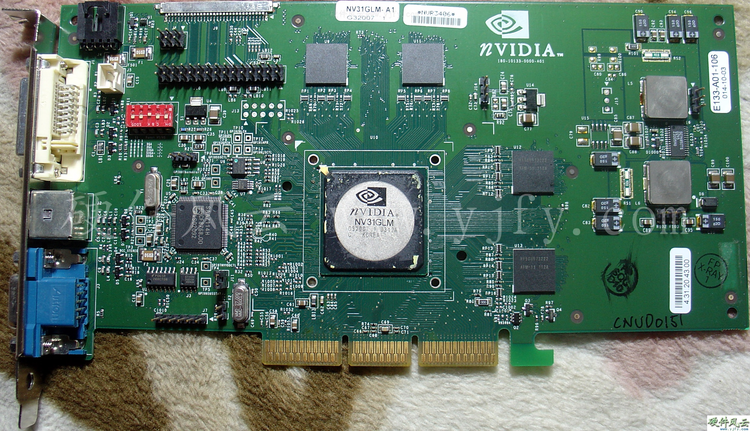
5.25 Quadro FX Go700
Model:E133
Chip model:NV31GLM A1
PCB Code:180-10133-0000-A01
2003��6��25�շ������ƶ��棬оƬ����0312�ܣ�PCB����0313�ܡ�
Quadro FX Go700 Engineering sample

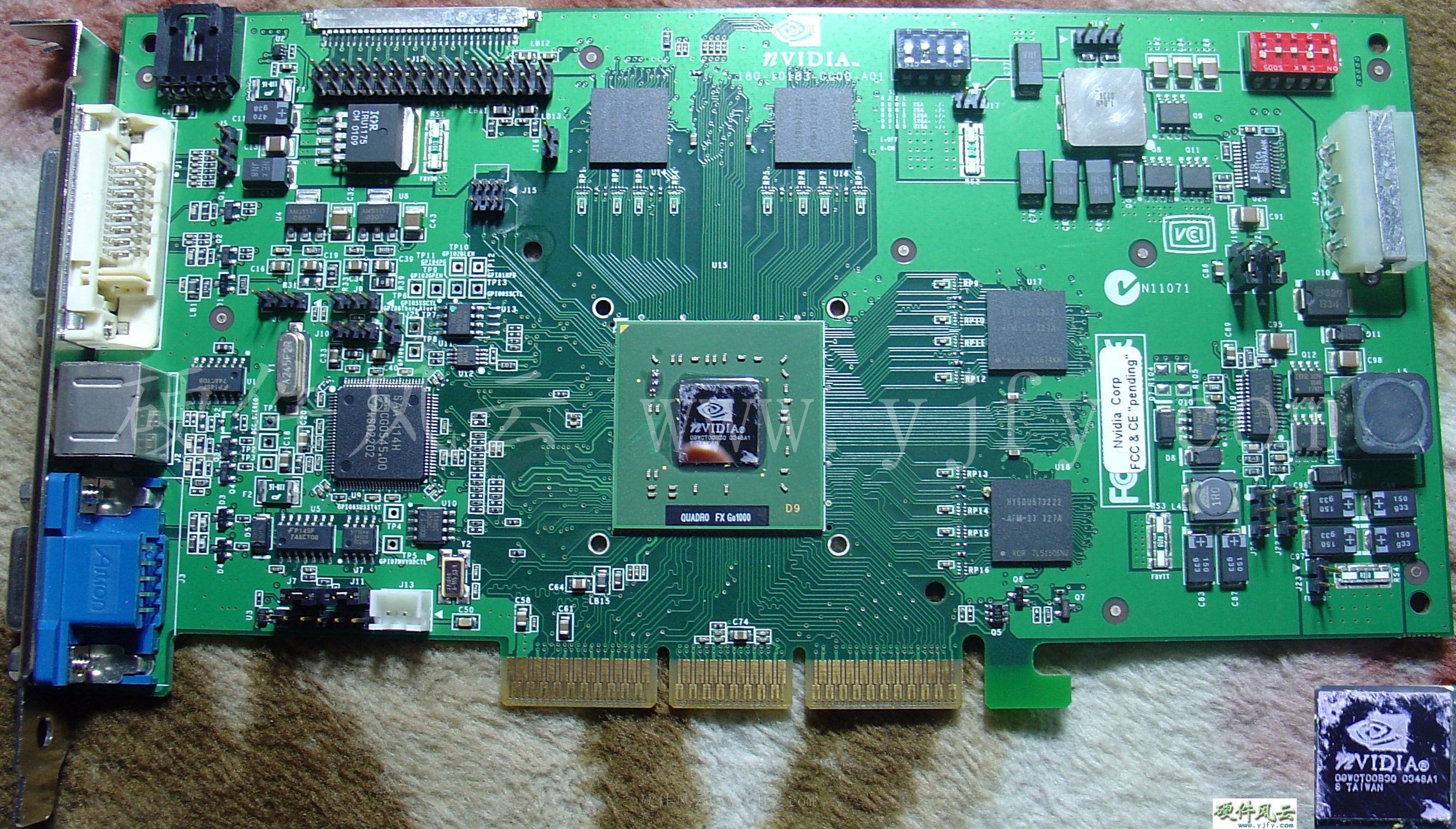
5.26 Quadro FX
Go1000
Model:E183
PCB Code:180-10183-0000-A01
Chip model:Go1000 A1
2004��2��25�շ�����
�ƶ��棬оƬ����0348�ܣ�PCB����0350�ܡ�
Quadro FX Go1000 Engineering sample

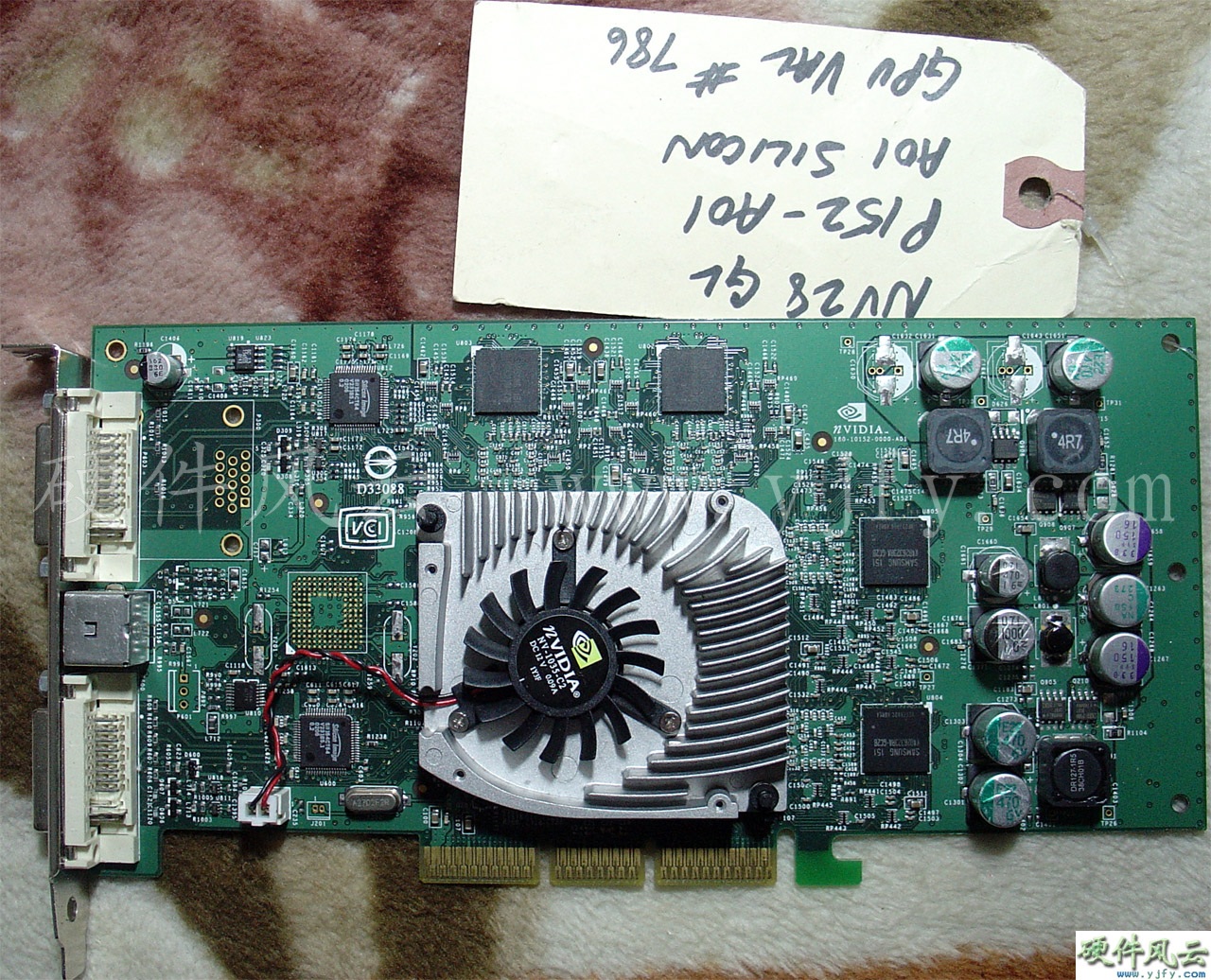
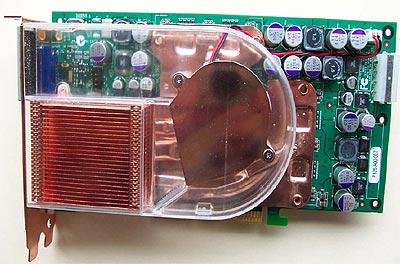
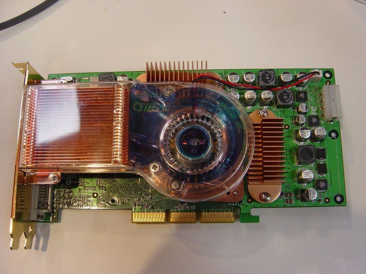
5.27 Abit
Siluro GeForce FX
5800ԭ�Ϳ�ʹ�õ���nVIDIA��T01ԭ�Ϳ�����
�����²�Ʒ��ʹ��"OTES III"ɢ��ϵͳ��
Siluro GeForce FX
5800 Engineering sample

��From
computerbase.de��
|


