|
Sample of computer hardware board
and card (3) Chip evolution
Intel i750 graphics card
evolution
This article commemorates the 30th anniversary of the release of
Intel's first graphics card
yjfy.com
Intel has produced
and sold display chips such as KU82706 and A82786 chips. Intel built
the i750 chip in December 1986 and was visualized by DVI (Digital
Video Interactive) Technology to develop the DVI Pro 750 graphics
card with the DVI (Digital Video Interactive) concept. DVI is an
all-digital sound, text, and graphics processing system that
supports multiple multimedia sources and information formats. Intel
is optimistic about this concept and is more optimistic about the
development prospects of digital multimedia technology. On November
14, 1988, it acquired the pioneer of digital media such as DVI
Technology. In March 1989, Intel Pro 750 was released. This is the
first graphics card that Intel officially released, and it has
entered the field of PC graphics.
The
Intel i750 graphics card project lasted for 6 years and it is
obvious that it is doing its best. In order to expand the impact,
even with the PC giant IBM. Unfortunately, in the era of the heroes,
Intel's efforts still have no breakthroughs, gradually disappeared.
So senior hardware enthusiasts only think that Intel's first
graphics card starts with the i740 chip...
This
article takes the unique INTEL i750 sample card and the
above-mentioned chip as an example, showing the long and arduous and
unknown process of computer chip and graphics card development,
trial production, trial production and mass production.
1. i750PA/DA Chip
1.1 About the i750PA/DA ES chip
Intel's i750 chip
consists of i750PA (82750PA pixel processor) and i750DA (82750DA
display processor). The technical parameters are: The 82750PA is a
25 MHz wide instruction processor that generates and manipulates
pixels. When paired with its companion chip, the 82750DA, And used
to implement a DVI Technology video subsystem, the 82750PB provides
real time (30 images/sec) pixel processing, real time video
compression, interactive motion video playback and real time video
effects.
Originally Intel's i750PA/DA chip was made in December
1986. In March 1987, a chip evaluation board for the
i750 chip, codenamed Tower, was made. The Intel Pro750
was released in March 1989 and will be available for
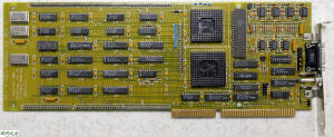
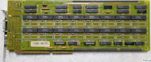
sale in July. The Intel Pro 750 consists of 3 cards
(Video, Audio, Utility) and 4 daughter cards (Video
Digitizer, Audio Digitizer, 2/4MB VRAM). The Intel Pro
750 Engineering sample collected on this site lacks a
video daughter card. The main card model of the Intel
Pro 750 is DVI VIDEO BOARD 02, and the PCB date is 8907.
It is the second version made by Intel after the
acquisition of DVI Technology on the DVI Pro 750 main
card DVI VIDEO BOARD 01 version. As shown below,
unfortunately there is no intel i750PA/DA chip.
Intel Pro 750
Engineering sample
When Intel
continued DVI Technology, a commercial-oriented Intel Pro 750
project, it also developed the ACTIONMEDIA series of graphics
cards for civilian use. ACTIONMEDIA literally understands that
it is universal media. The first generation of ACTIONMEDIA
graphics card is the commercial digital media development
technology of the Intel Pro 750 to the ACTIONMEDIA 750 DVI for
civilian consumption digital multimedia graphics. The product
development code for the ACTIONMEDIA 750 DVI is DS1, which is
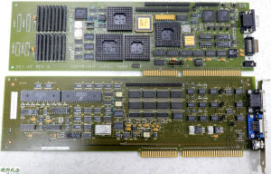
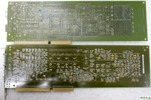
paired with the CS1 secondary card. The following DS1-AT is an
ISA interface Product Evaluation board. Although the main chip
of this board is missing, the chip used in this board is the
same as the chip used in the ACTIONMEDIA 750 DVI product test
board. It can be known that the missing chips are Intel
i750PA/DA and VLSI VTG8001/8002.
DS1-AT
Product
Evaluation board


DS1-AT + CS1AT
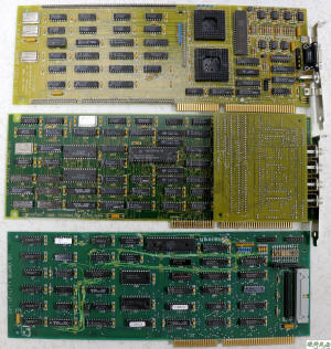
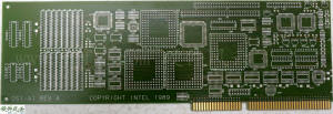
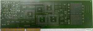
The board below is a
blank PROTOTYPE board without a chip.
DS1-AT
PROTOTYPE board
The i750PA/DA chip of
the engineering sample version has been hidden by Intel. Is the
official version of the i750PA/DA chip looking for it? In the
past, whether it was Intel Pro 750 or ACTIONMEDIA 750 DVI, "Only
available in limited quantities", even when it was a picture of
these products, it was not easy, let alone the drawings of
engineering samples. Thanks to the computer hardware collection,
I have not seen it in the past, but now I can have it!
1.2 i750PA/DA Chip
The ACTIONMEDIA 750 DVI
attracted widespread attention after its display at the COMDEX/Fall
'89 show from November 13 to 17, 1989. Officially released in March
1990.
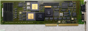
The following is the
engineering sample of ACTIONMEDIA 750 DVI, the official version of
the i750PA/DA chip, the chip production date from 8930 to 9044, the
time span of more than one year. The first one was an earlier
unproductive Product Test board with a chip date of 89 years.
ACTIONMEDIA 750 DVI
Engineering sample
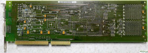
The second is also an
unproductive product test board, except that the chip dates above
are 90 years. With a CS1AT sub-card from the CSCAT sub-card sticker
"FCC CLASS A" can be seen, this product is not suitable for home, it
can be seen that this product is still no retail.
ACTIONMEDIA 750 DVI
+
CS1AT
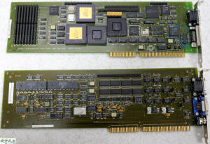
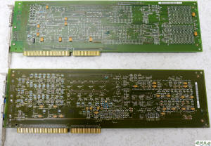
The
third is the engineering sample of the MCA interface
version ACTIONMEDIA 750 DVI. The chip is late, the chip
date is 9044, about 90 years in October, and half a year
after the release date of March 1990, it can be seen
that it was difficult to produce for some reason.
ACTIONMEDIA 750 DVI MCA
+ DS1MCA
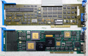
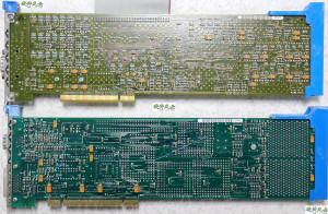
The MCA interface
ACTIONMEDIA 750 DVI once appeared on behalf of the ACTIONMEDIA
series on March 5, 1990, "INFO WORLD", the only ACTIONMEDIA 750
DVI picture that can be seen on the Internet.
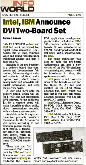
2.
i750PB/DB ES Chip
In the late 1980s,
the patch manufacturing process of the board was mature, and intel
was naturally the leader. The i750PA/DA chip of the PGA pin
structure is upgraded to the i750PB/DB chip of the PQFP chip
structure, and the chip package is changed from a gold seal to a
plastic package. Based on the mature design of the previous
generation, the chip evaluation board INTEGRATOR was developed. So
the INTEGRATOR looks like the ACTIONMEDIA 750 DVI for the chip, or
the CS1 card.
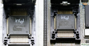
The ISA interface version
of the detachable Chip Evaluation board INTEGRATOR's two i750PB/DB
chips are ES.
INTEGRATOR
Chip
Evaluation board
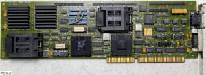
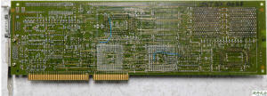
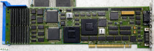
The figure below shows the INTEGRATOR of the MCA
interface version. The i750PB/DB ES chip date is very
early, it is 9014/9017, and the two chips are a step.
The ES chips for b step and c step will also appear in
the card below.
INTEGRATOR MCA
Chip
Evaluation board


The release date of
the ACTIONMEDIA 750 DVI was officially released in March 1990.
From the above figure i750 chip date 9014, it can be seen that
at least on the ACTIONMEDIA 750 DVI release date, Intel began to
work on the development of ACTIONMEDIA II. The unsuccessful
ACTIONMEDIA 750 DVI has a lot to do with Intel's lack of effort
in making this project a transition. The INTEGRATOR of the MCA
interface above has another unusual point, that is, most of the
chips on the card may be blacked out due to confidentiality.
Obviously it has been shown, it is estimated to pull the IBM
cooperation together with the deputy card to demonstrate the
feasibility of the project.
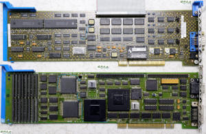
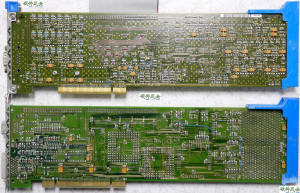
MCA Interface Version
The secondary card of the INTEGRATOR is the secondary card
CS1MCA that directly uses the previous generation ACTIONMEDIA
750 DVI.
INTEGRATOR + CS1MCA
3.
i750PB/DB+i750LA/LH/LV Chip
ACTIONMEDIA II was released on October 17, 1991 and was exhibited at
COMDEX Fall '91 on October 21-25, 1991 and won the Best of Show
Award and Best Multimedia Product Award.
Intel's ACTIONMEDIA II graphics card is to further optimize the
structure of the ACTIONMEDIA 750 DVI primary and secondary cards as
the main daughter card structure, and also designed three
QFP-structured i750 series auxiliary chips for the i750PB/DB chip.
These 5 chips are:
82750PB pixel processor
82750DB display processor
82750LA Keying and Audio Gate Array (KAGA)
82750LH Host Interface Gate Array (HIGA)
82750LV VRAM SCSI Capture Gate Array (VSCGA)
3.1 ES Chip
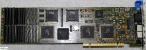
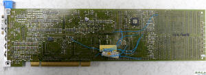
The ACTIONMEDIA II
Product Evaluation board is codenamed DS2. The following MCA
interface version ACTIONMEDIA II is DS2MCA, which has five i750
chips. The i750PB/DB is obviously the ES version. The only three
codes of the ceramic seal are not the unlabeled models. It is the ES
chip of the early i750LA/LH/LV.
DS2MCA
Product Evaluation
board
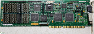
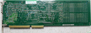
The following ISA interface version ACTIONMEDIA II is DS2AT. The
above i750PB is not an ES chip, the i750DB and three
i750LA/LH/LV are plastic ES chips.
DS2AT
Product Evaluation board
3.2
Official
Chip
The chip has two types of
annotations, one is LA, LH, LV, which is an early label.
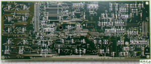
DS2MCA
Product Evaluation board/PROTOTYPE
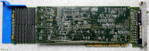
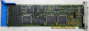
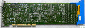
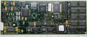
CS2 daughter
card Engineering sample
The
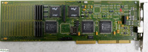
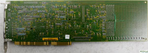
other labels are S82750LA, S82750LH, and S82750LV.
Smart video Recorder
Engineering sample
For more ACTIONMEDIA II graphics cards see:Sample
of computer hardware board and card (2)
Board type
4. i750PB/DB+i750SN(F119902HFEX/F122164HFEX)ES Chip
Around 92 years, Intel began to develop the next generation of
products, let's call ACTIONMEDIA III, ACTIONMEDIA III is also the
main card daughter card structure. In ACTIONMEDIA II, the main card
is five i750 series chips, and the main card of ACTIONMEDIA III is
reduced to three i750 series chips. The daughter card is reduced
from two rows of sockets to one socket. This information is not
released by Intel, but from the two Engineering sample cards
collected on this site.
ACTIONMEDIA III should update the i750PB/DB and launch the
i750PC/DC Chip Evaluation board. In fact, it is an evaluation of the
update of the auxiliary chip. Presumably, the chip to be evaluated
integrates the functions of the original 82750LA, 82750LH, and
82750LV3 chips. The chip to be evaluated should be i750SN, which
will be introduced later.
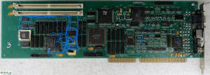
I once thought that these two cards are ACTIONMEDIA III
Product Evaluation boards, but half of the space on the board is
occupied by the plug-in seat, and the product evaluation board is
very close to the final product, which is obviously the Chip
Evaluation board, codenamed QUARK.
The following QUARK ceramic seal ES chip is F119902HFEX, the
production date is 9241.
QUARK
Chip Evaluation board
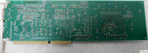
The following QARK
1.5 ceramic seal ES chip is F122164HFEX, the production date is
9309.
QUARK
1.5
Chip Evaluation board


5.
i750PB/DB+i750SN(F122164PPM)ES+TC160G54ES
Chip
QUARK's REV
2 version compared with the above REV 1 version, QUARK's REV 2
version of the chip evaluation board is about one-third wider than
the REV 1 version of the standard ISA full-length board, the extra
place is loaded two One function, one on the right, is the function
chip evaluation board area of the daughter card, and the function
of the daughter card is directly extended on the main card. As the
integration level is improved and the memory is processed in two
slots, the ISA interface master card has enough functions to
directly accommodate the daughter card, and the daughter card
function can be cut by the empty soldering; the MAC interface
version is small. This sub-card may be used, but IBM has now given
up on the exclusive MCA interface and turned to the universal PCI
interface invented by Intel. The daughter card has become redundant.
It can be said that the PCI interface standard completely ended
Intel's own ACTIONMEDIA series of graphics cards. The PCI standard
was developed by Intel around 1990. On June 22, 1992, Intel released
the PCI 1.0 standard, which is limited to component-level
specifications. On April 30, 1993, the PCI-SIG released the PCI 2.0
standard, which for the first time created the standard between the
connector and the motherboard slot. Later, with the assistance of
Intel, ATI took the lead in releasing the first PCI graphics card in
history. Interested to see this link:
http://www.yjfy.com/Museum/video/MACH32_PCI_ES.htm
The picture below is the earliest PCI interface card in history,
date is 1290 (12th week of 90).
PCI interface PROTOTYPE
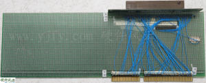
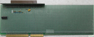

As can be seen from the serial number of the ACTIONMEDIA II product,
the ACTIONMEDIA II series only produced tens of thousands of pieces
in total, which shows that it was unsuccessful. Even though Intel
wants to use IBM's influence, marking ACTIONMEDIA 750 DVI and
ACTIONMEDIA II with "JOINTLY DEVELOPED BY INTEL AND IBM" still has
little effect. In fact, the cost of the all-round digital media
graphics card is too high. The most important thing is that the i750
chip is designed in 1986. It is a big problem to change the PCI
interface. Therefore, the failure of this ACTIONMEDIA III project is
also a matter of time. At this point, Intel has gradually abandoned
the PC graphics market.
Let's take our eyes back to QUARK's REV 2 version of QUARK II
and QUARK 2.5, with a socket on the left and an external interface.
This feature is related to "programmable logic." A program error is
found in the design of the logic circuit in the prototyping stage
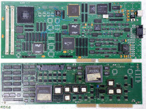
for the development process, and the error is corrected. The
matching DVI THUMPER secondary card can be connected to the main
card through the cable. This interface has not been made on the
collection of QUARK II and QUARK 2.5 graphics cards.
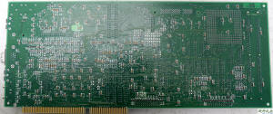
5.1 i750PB ES/i750DB+F122164PPM Chip
The chip evaluation board QUARK II chip in turn i750PB C-STEPPING
ENG SAMPLES, i750DB, F122164PPM, and an empty soldering chip related
chip will be introduced below. This F122164PPM is a plastic ES chip,
which is later than the ES chip of the ceramic seal F122164HFEX on
the REV 1 version of QUARK.
QUARK
II
Chip Evaluation board
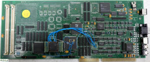
5.2 i750PB/i750DB+F122164PPM+TC160G54ES Chip
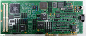
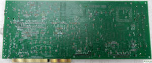
Chip
evaluation board QUARK 2.5 chip in order i750PB, i750DB, F122164PPM
and TC160G54ES, this TC160G54ES chip is very special, Intel not only
set a PGA chip socket on the graphics card, but also equipped with a
DVI THUMPER secondary card to deploy. This interface has not been
made on the QUARK 2.5 graphics card, but the above socket can be
indirectly debugged using Altera's EPM7192GC160-1 PGA chip that has
been processed by the DVI THUMPER secondary card.
QUARK
2.5
Chip Evaluation board
QUARK
2.5 +
DVI THUMPER
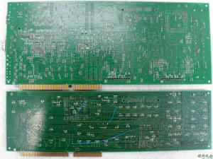
6. i750PE
ES + i750DB + i750SN Chip
Due to the
large investment in the i750 project, it is still wise to say that
Intel has begun to return to the position of chip manufacturing
sales. Intel temporarily bid farewell to the graphics card field,
but did not completely abandon the research and development of the
i750 chip follow-up products, turned to simplified functions,
low-cost video daughter cards and committed to selling i750 series
chips to large companies such as ATI and
Creative.
The research and development project codenamed MAESTRO is an
attempt to enter the single-function video daughter card field after
Intel abandoned the all-round digital media ACTIONMEDIA series
graphics card. After watching the luxury lineup of the i750 graphics
card, look at the MAESTRO III below, it is really difficult to hook
up with the Intel i750 graphics card on the tall.
MAESTRO III
Engineering sample
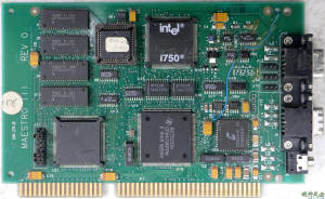
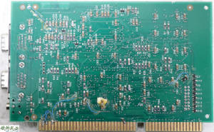
The MAESTRO III card
has i750DB, i750SN and a chip without any label. This chip
without any standard should be the next generation chip, because
at this time Intel can not make the i750PB into a wordless
version of ES. The i750SN chip should be the F122164PPM on the
QUARK chip board.
For some reason, this card was not sold at the end. Perhaps
the price/performance ratio is lower than those on the market.
7.
i750PE+BORG+CGA Chip
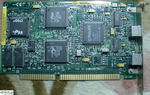
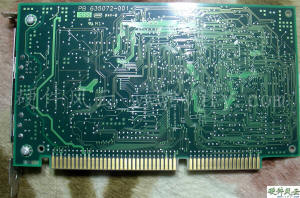
The card with the FCC ID
EJMPCVD11XX is an official product of Intel. The official name is
called SMART VIDEO RECORDER PRO or SMART VIDEO RECORDER PRO II. But
one thing is certain, it uses the research results of the two chip
evaluation boards, QUARK and MAESTRO. The chips on EJMPCVD11XX are
i750PE, BORG, CGA, among which: i750PE is from the wordless i750
chip on MAESTRO III, based on i750PB, the frequency is 25 Mhz like
i750PE; BORG is from iESTSN of MAESTRO III; CGA is from QUARK 2.5
The TC160G54ES chip; EJMPCVD11XX has no VGA interface, so the i750DB
(82750DB display processor) chip is not required.
SMART VIDEO RECORDER PRO
Official
Product
8.
i750PD ES Chip
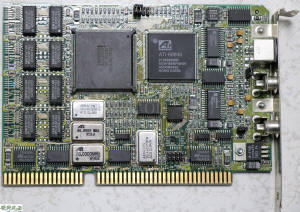
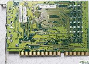
On
November 15, 1993, ATI announced the Video basic capture card, which
uses Intel's low-cost i750PD and ATI's ATI-68890 video capture chip.
The chip below shows the ATI Video basic capture card is ES, the
chip is labeled KU8270PD-25, it seems to be marked incorrectly, it
should be KU82750PD-25. Retail products rarely use ES chips even in
the early days, and the use of ES chips in mid-to-late products is a
violation, especially in the official products of large
manufacturers, such violations are rare.
ATI
Video basic
capture card
Official
Product
The i750 chip project began in 1986 with
the i750PA/DA chip, and finally the 1993 i750PD chip, which
lasted 8 years. The i750 chip was undoubtedly excellent at the
beginning of its birth. Intel did not update or replace the PCI
interface. In the latter stage, its excellent performance index
became a congenital deficiency. In the end, it had no potential
to be dug and had to end. The 2D graphics project of Intel's
i750 chip is also finished. As for the later 3D graphics card,
the i740 chip graphics card developed by Intel and Real3D in the
second half of 1997, see:
Sample of computer hardware board and card (1) versions definition
|