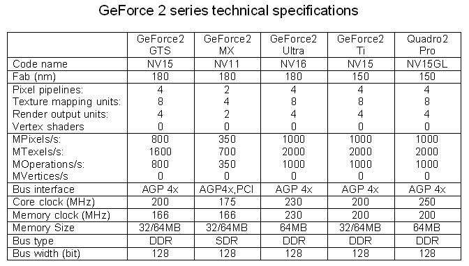
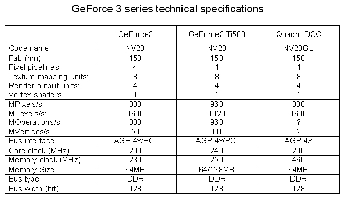
|
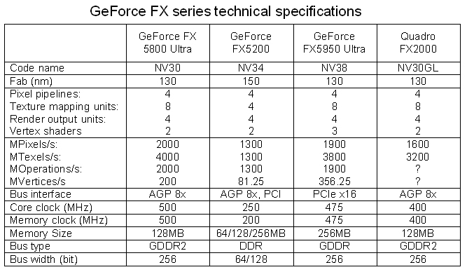
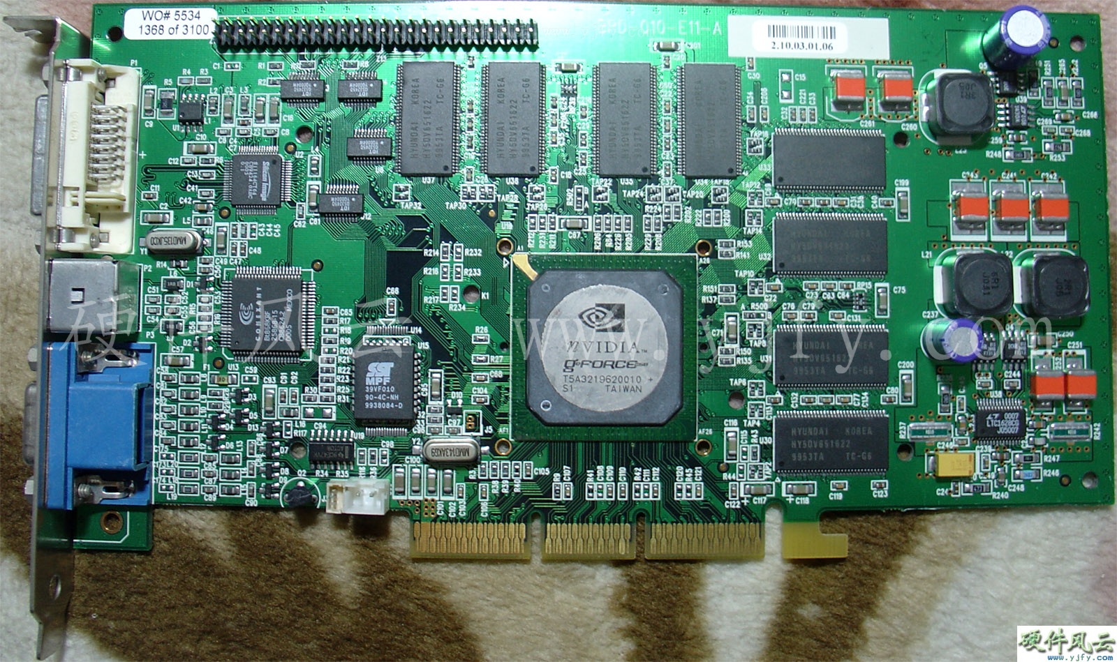
5. GeForce FX(NV30)series
After repeated delays,
nVIDIA released the GeForce FX5800/5800 Ultra graphics cards on November
18, 2002, and the actual release date was in March of the following
year. The NV30 chip is made with 130 nm transistors, operates at a
frequency between 400 and 500 MHz, and can access 128MB GDDR2 via a
128-bit bus running at 800 MHz or 1000 MHz.
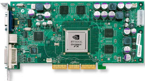
GeForce FX5800 Ultra Engineering
sample
One of the reasons why
GeForce FX uses "FX" instead of the number "5" is that many former
engineers of 3dfx have participated in the development of GeForce
FX. Due to the incomplete realization of the innovative design, and the
imperfect GDDR2 memory. This causes the GeForce FX5800/FX5800 Ultra
graphics cards to generate a lot of heat. The performance barely
surpasses the Radeon 9700 Pro (R300 series) that made the limelight in
2002.
On March 6, 2003, ATi released the Radeon 9800 Pro.
It is a version that optimizes the Radeon 9700 Pro, increases the
frequency, and can well support GDDR2. Its performance exceeds the
GeForce FX5800 Ultra graphics card.
Radeon 9800 Pro

(From ixbt.com)
Radeon 9800 Pro caught nVIDIA
by surprise. I had to give up the immature GDDR2 video memory for the
time being. On May 12, 2003, it released the GeForce FX5900 Ultra, which
uses GDDR1 video memory, and has improved graphics quality, heat
dissipation, and power consumption. This enables GeForce FX5900
Ultra/FX5950 Ultra to compete with Radeon 9800 Pro/9800 XT graphics
cards.
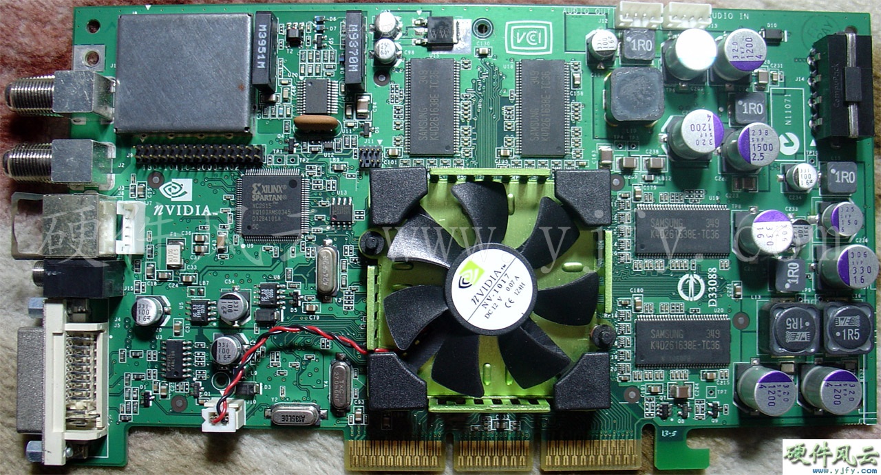
On June 13, 2003, Xabre Graphics (XGI), a newly
established subsidiary of SiS, acquired Trident’s graphics chip
development business at an undisclosed price. On September 15, 2003, XGI
announced the Volari V3/V5/V8 chip graphics card and the Volari Duo V8
Ultra graphics card with dual display chips. Among them, the Volari V3
graphics card is the Trident XP5 graphics card, and the Mobile Edition
is called Volari XP5. The performance of Volari Duo V8 Ultra graphics
card is slightly higher than that of GeForce FX 5700 Ultra, and sales
are less. Because of its powerful appearance created by its dual display
core, it is now the darling of collectors.
Volari Duo V8 Ultra Engineering
sample
The second product in VIA’s Chrome product line is DeltaChrome S8, which
was not developed smoothly. S3 designed the DeltaChrome S8 evaluation
board in August 2003, and it was not officially released until July 28,
2004. It supports DirectX 9a, and its 3D processing capability is close
to that of the mid-level graphics card FX 5700Ultra at that time.
DeltaChrome S8 Engineering
sample

(From legitreviews.com)
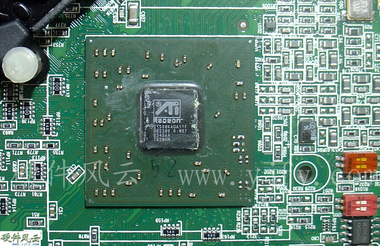
On July 23, 2002, Intel supported AWG (Arapahoe Work
Group) officially released the PCI Express computer bus, referred to as
PCI-E, and officially referred to as PCIe. Due to the close cooperation
between ATi and Intel, it was the first to showcase the industry's first
graphics card using PCI Express at IDF2003 on September 19, 2003 (week
0338). The specific model of this card was not announced. The chip shown
in the picture is labeled "215S8KAGA11F", which has integrated PCI-E. It
is an engineering sample chip of RV380 (X600). It can be seen that the
first graphics card in the industry that uses PCI Express is Radeon
X600, and the PCB date is 0330 weeks.
Radeon
X600
Engineering sample

Since the publication
of the PCI Express interface standard, nVIDIA's R&D pace has lagged. The
solution is to design the AGP-to-PCI Express bridge chip BR02. BR02
stands for Bridge Revision 02, also known as High Speed Interconnect (HSI).
It can convert AGP signals to PCI-E signals, and it can also convert
PCI-E signals to AGP signals. On February 17, 2004 (0408 week), nVIDIA
released the GeForce PCX series of graphics cards using the BR02 chip.
The BR02-A1 ES chip in the picture is dated 0345 weeks. It seems to feel
the huge pressure of ATi and accelerate the finalization. The BR02-A2 ES
chip has a date of 0407 weeks and is finally finalized in A2.
GeForce PCX5300
Engineering sample
GeForce
PCX is mainly based on the unsuccessful old product GeForce FX series,
and its conversion performance will be slightly lost, so the bridge chip
has been criticized. ATi also said: "Where is there a way to build a
bridge". In the period of GeForce 6 and GeForce 7, the advantage of the
BR02 chip finally emerged, that is, only one interface chip needs to be
developed. ATi chips are all native, that is, a single chip launches
native PCI-E and native AGP versions at the same time. Finally, due to
cost pressures, the Rialto unidirectional bridge chip that converts
PCI-E signals to AGP was also developed.
The embarrassing situation of nVIDIA's lagging behind
PCI-E interface graphics cards in desktop computers prompted it to
cooperate with many notebook computer manufacturers to announce the
mobile PCI Express Module (MXM) specifications for notebook computers on
May 17, 2004. The full name of MXM technology is Mobile PCI eXpress
Module.
GeForce PCX5300 MXM Engineering sample
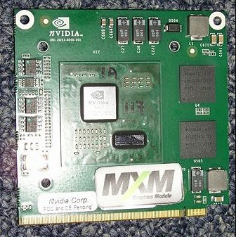
(From hexus.net)
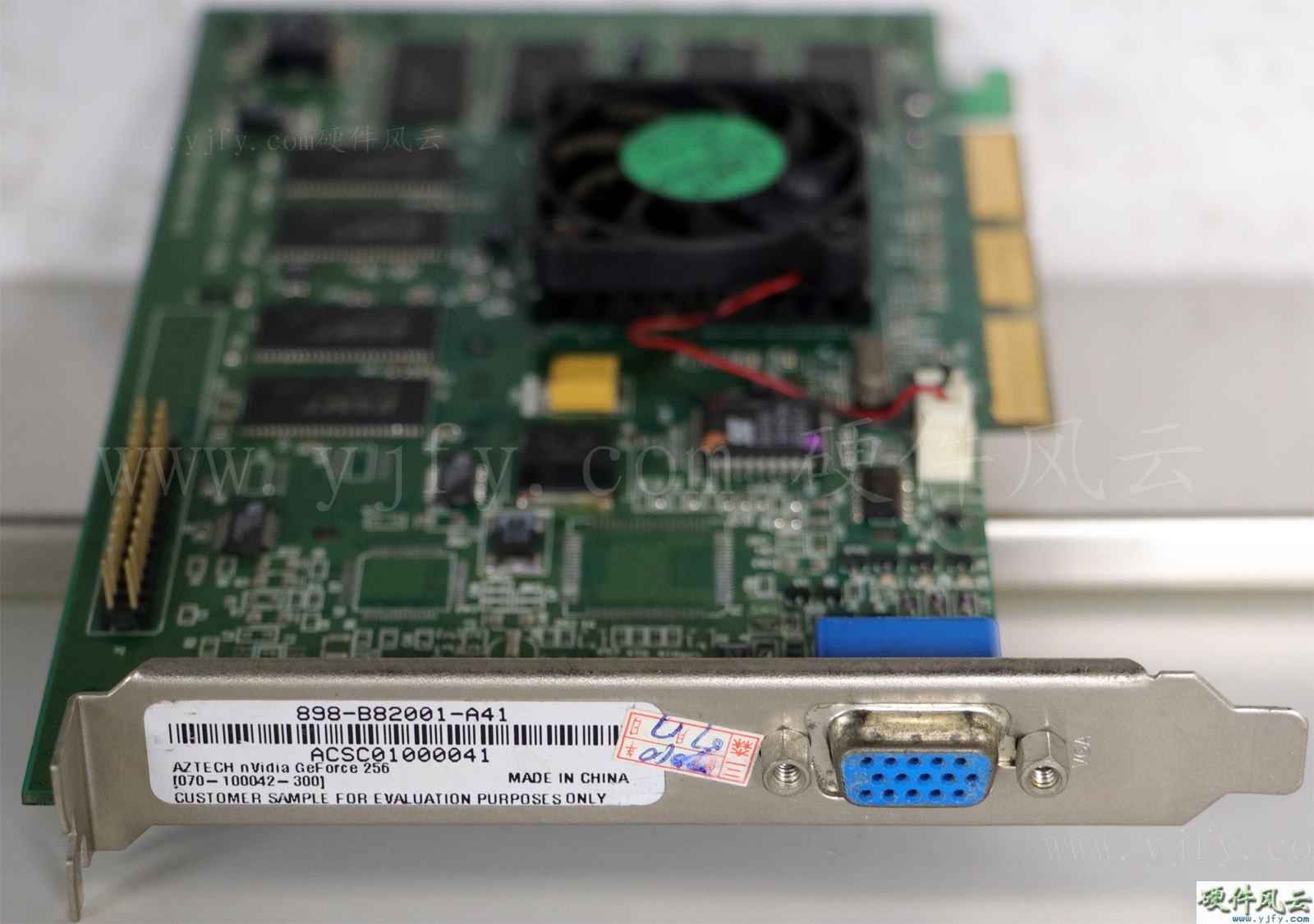
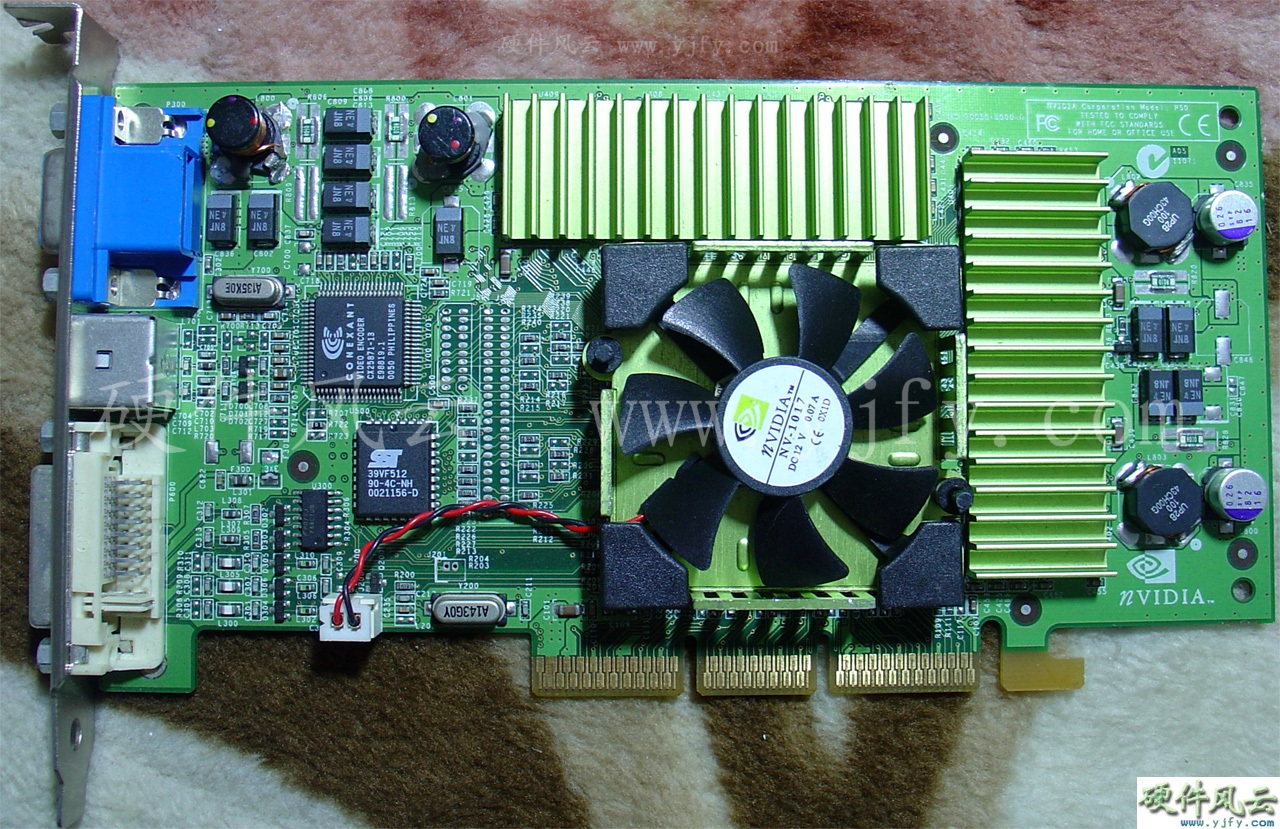
nVIDIA also released the entry-level and mid-range versions
of GeForce FX: mid-range FX5600 (NV31), FX5700 (NV36) and entry-level
FX5200/5500/5100 (NV34), as well as the corresponding mobile version.
5.1
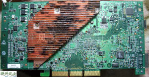
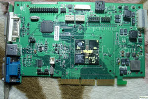
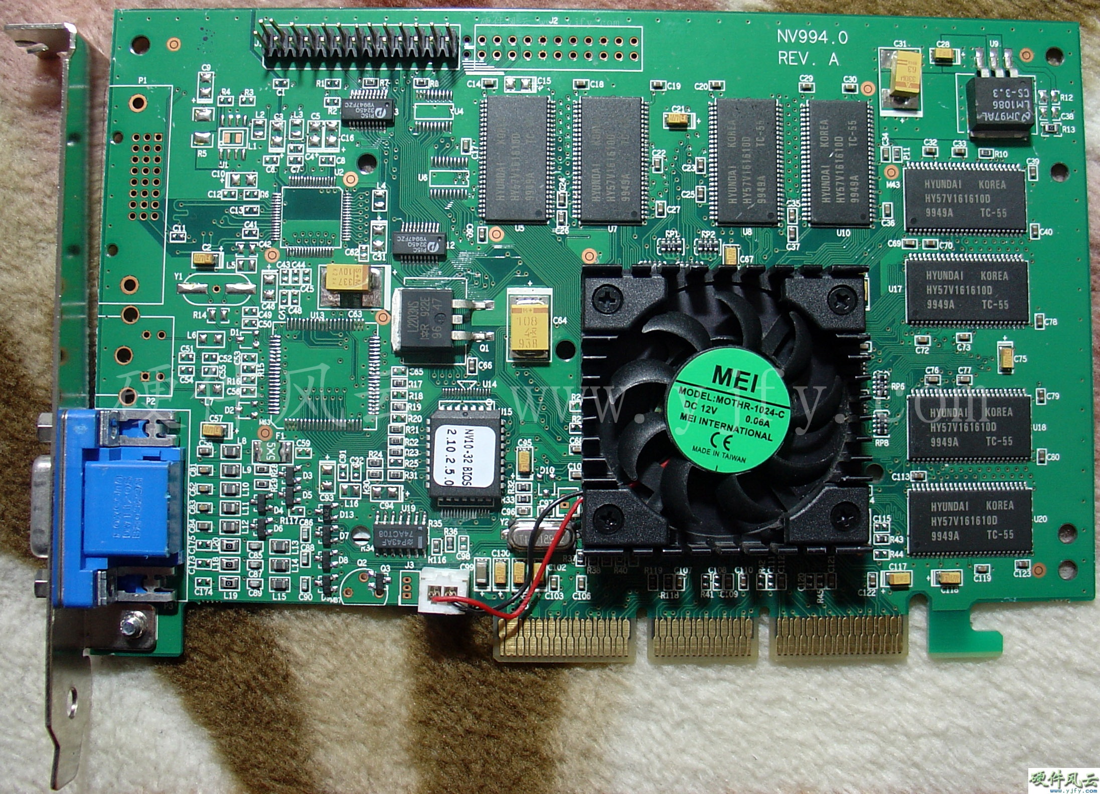
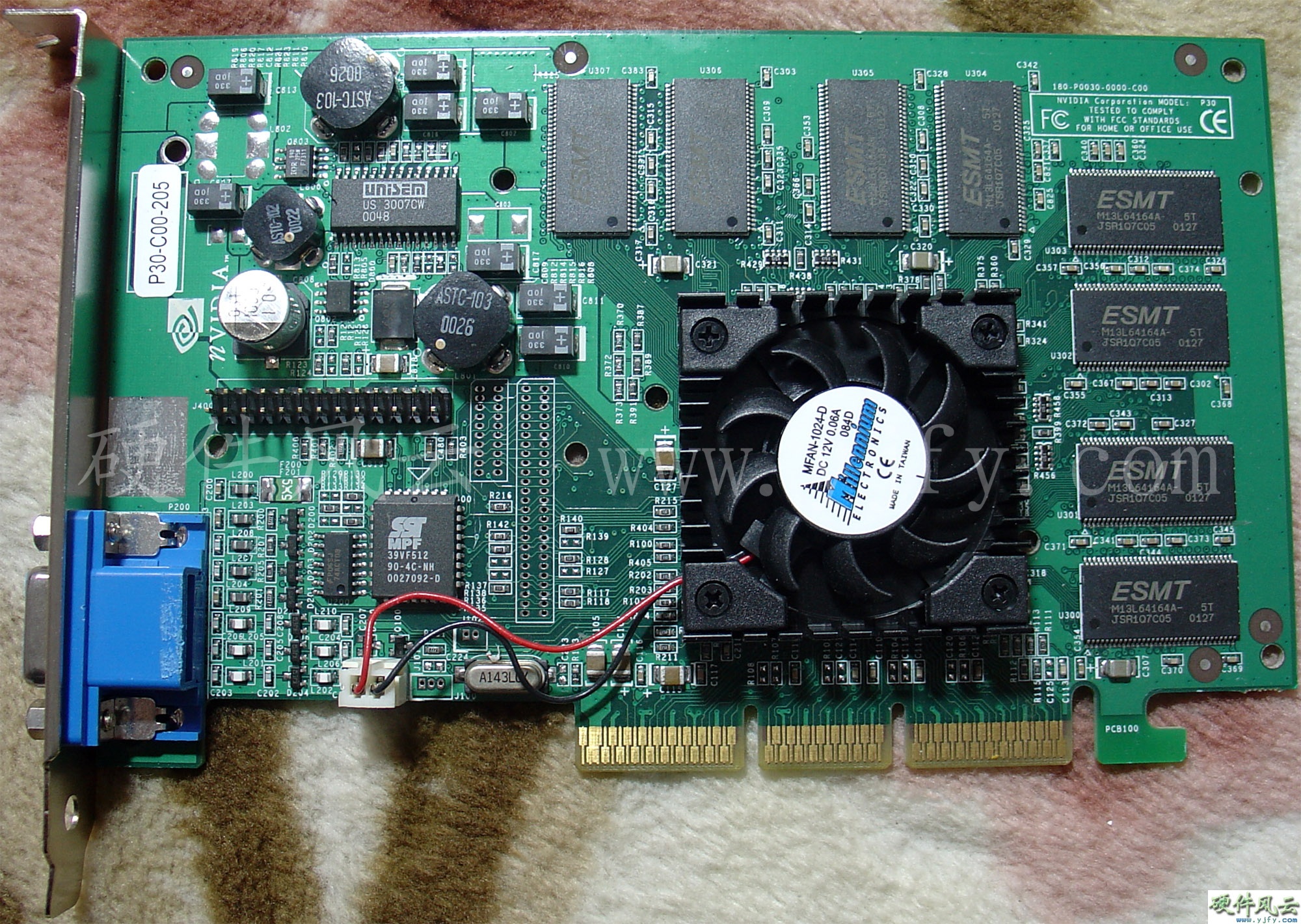
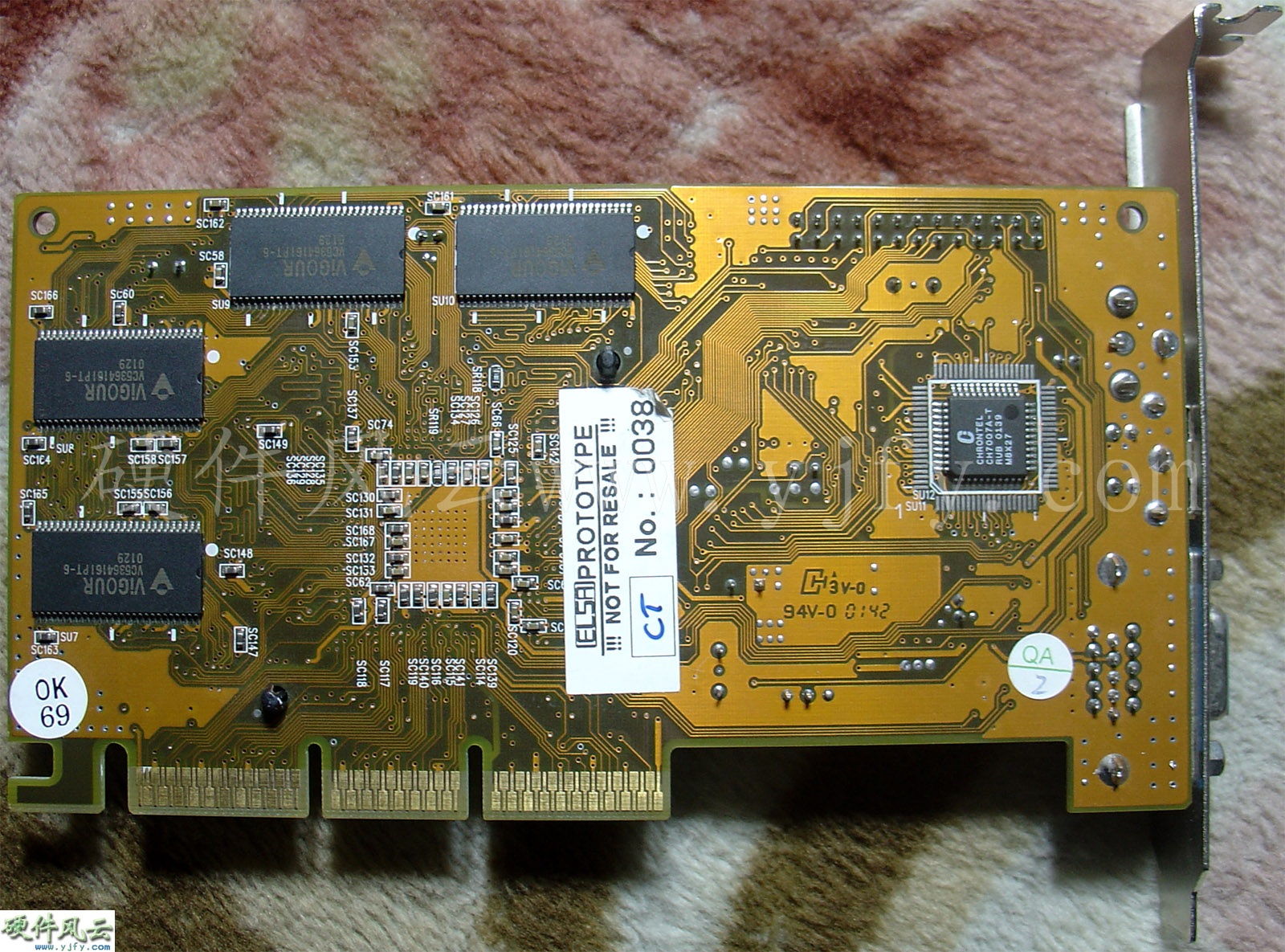
GeForce FX5800/FX5800 Ultra
5.1.1 Rev A00
There are two types of
Rev A00 from GeForce FX, T01 using GDDR1 video memory and P126 using
GDDR2. There is no difference between T01 and P126 from the front,
except that the capacitor used by T01 is slightly smaller.
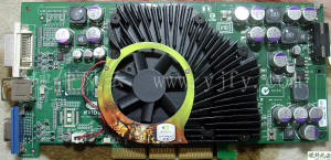
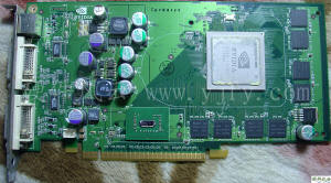
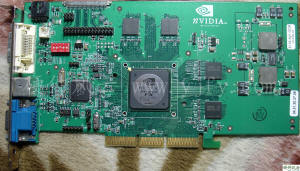
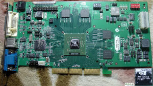
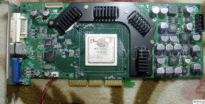
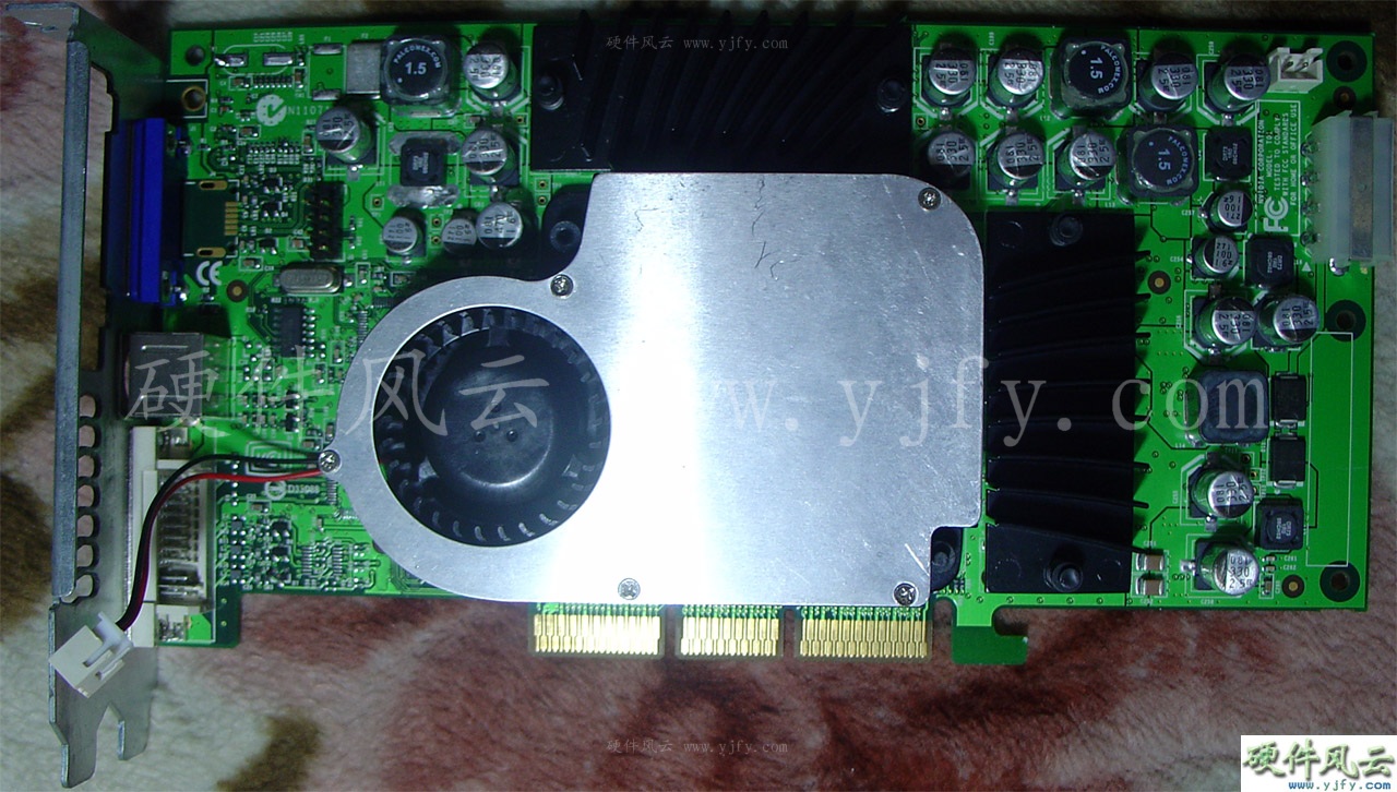
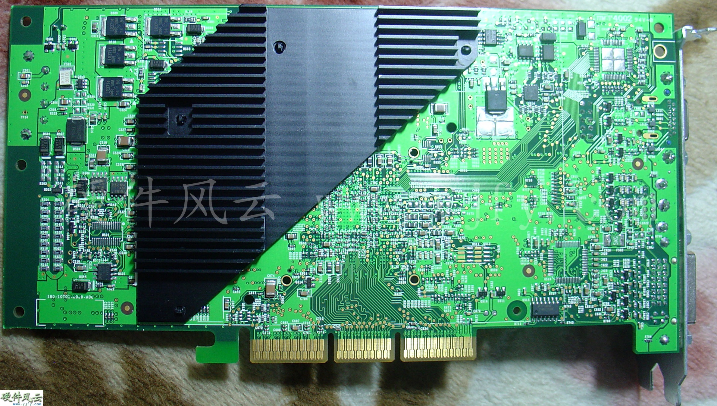
5.1.1.1 T01
PCB Code:180-10T01-0000-A00
At the beginning of
August 2002, the first NV30 silicon taped-out. It takes about 4 weeks
(0236 weeks) to package the chips, and 4 weeks (0240 weeks) to test the
chips. The PCB date of this T01 is 0240 weeks, which should be the
earliest version. The NV30 chip on the PCB is the first packaged chip,
and the chip is marked as follows:
TMG177-12"-PI8124(12
inch wafer)
N91517.06(Unknown)
EHS-FCBGA
1152(External Heat Spreader Flip Chip BGA 1152 Pin)
Ibiden Daisy
Chain(Ibiden Co Ltd ,Daisy Chain Topology)
T01 is a chip evaluation
board for NV30 chip, using mature and reliable MBGA package GDDR1 video
memory. After the verification is feasible, directly copy the P126
product evaluation board/reference board using GDDR2 video memory.
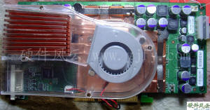
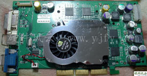
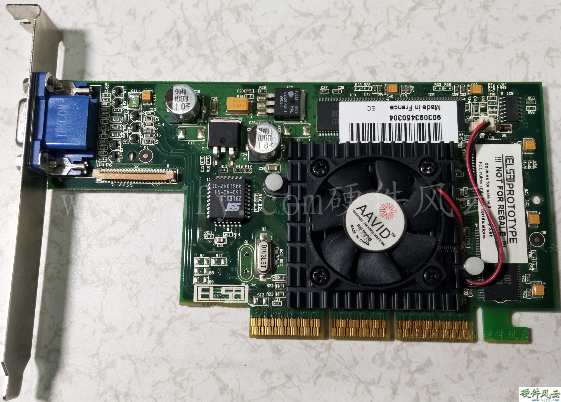
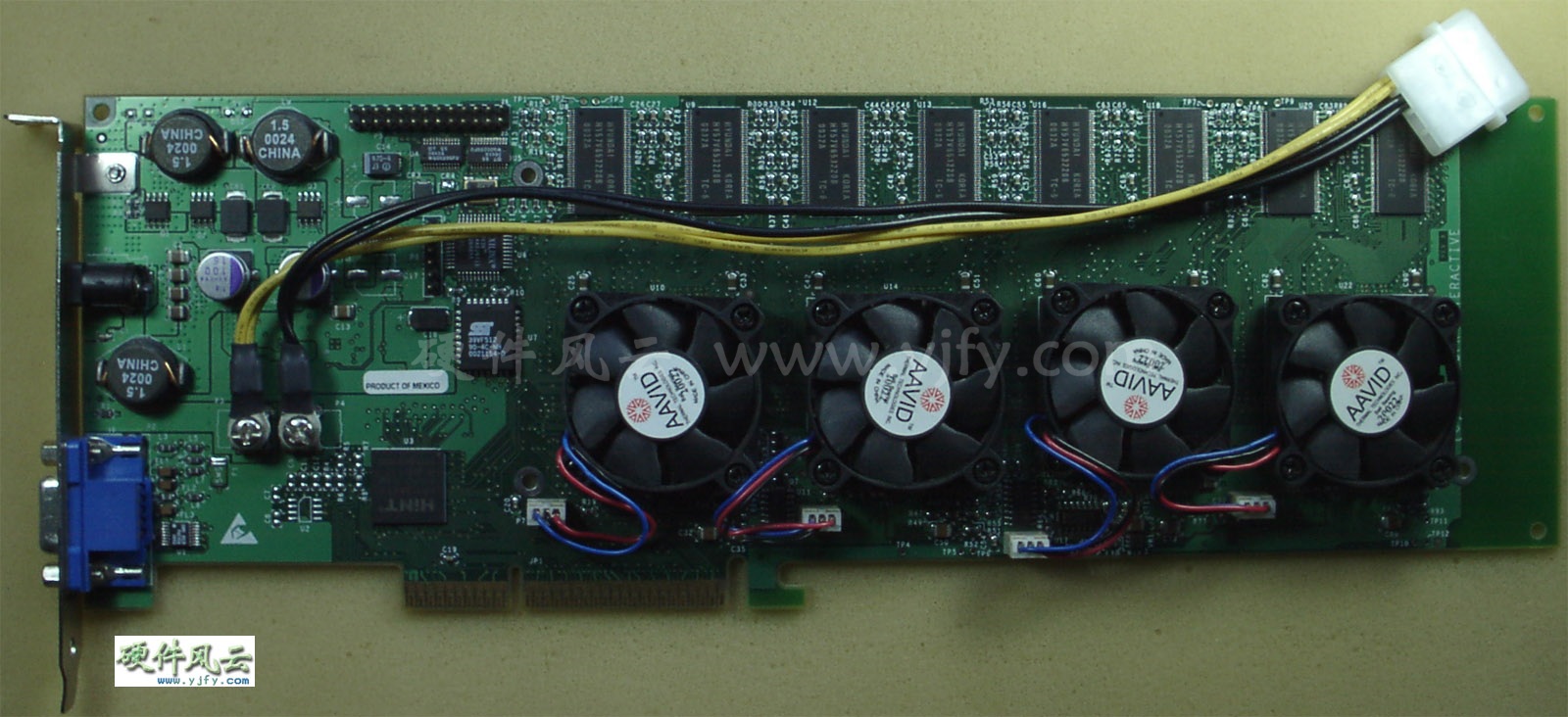
The cooling system is the prototype of GeForce FX5800
(QUADRO 2000). The fan power cable is in the lower left corner, and the
length is not enough to plug into the upper right socket. The lower left
socket is blocked by the heat sink. It was pasted with glue on the lower
left fan socket 3 cm to the left. Suspected exhibit samples.
GeForce FX5800 Engineering
sample

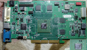
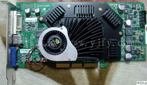
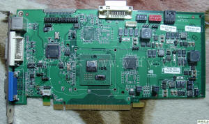
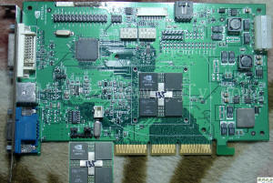
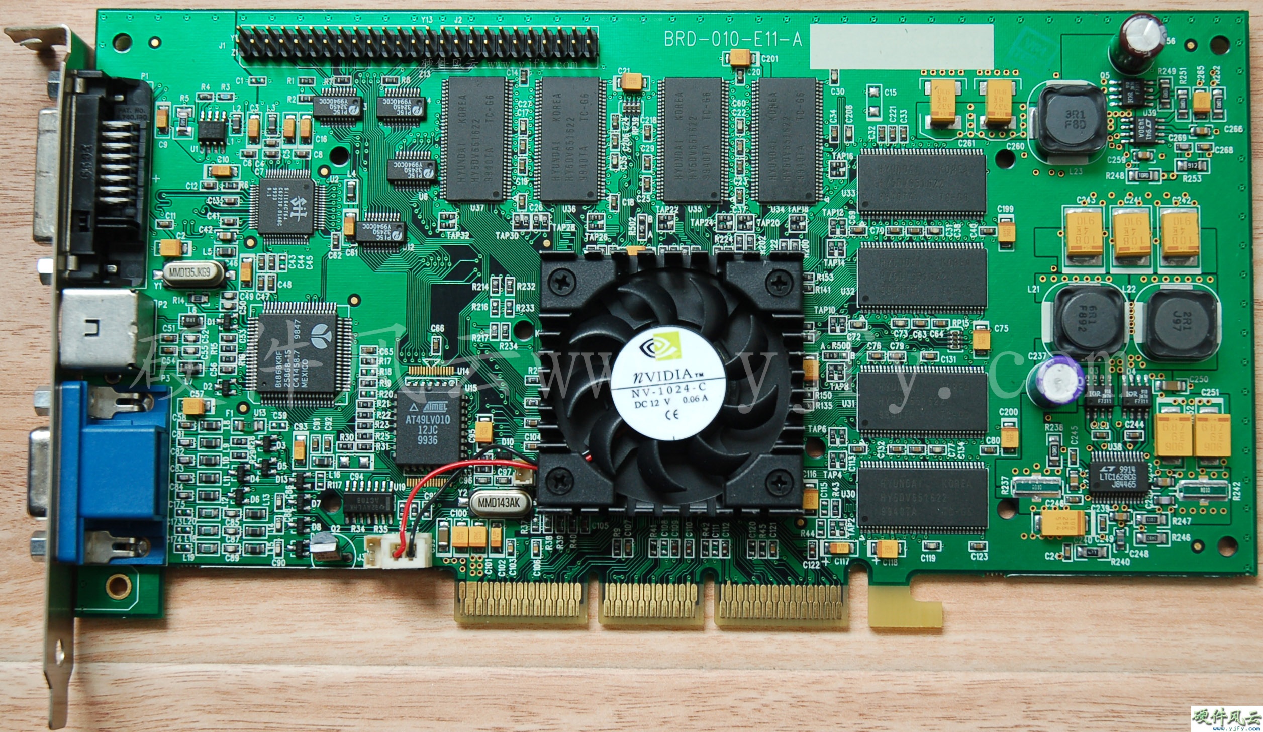
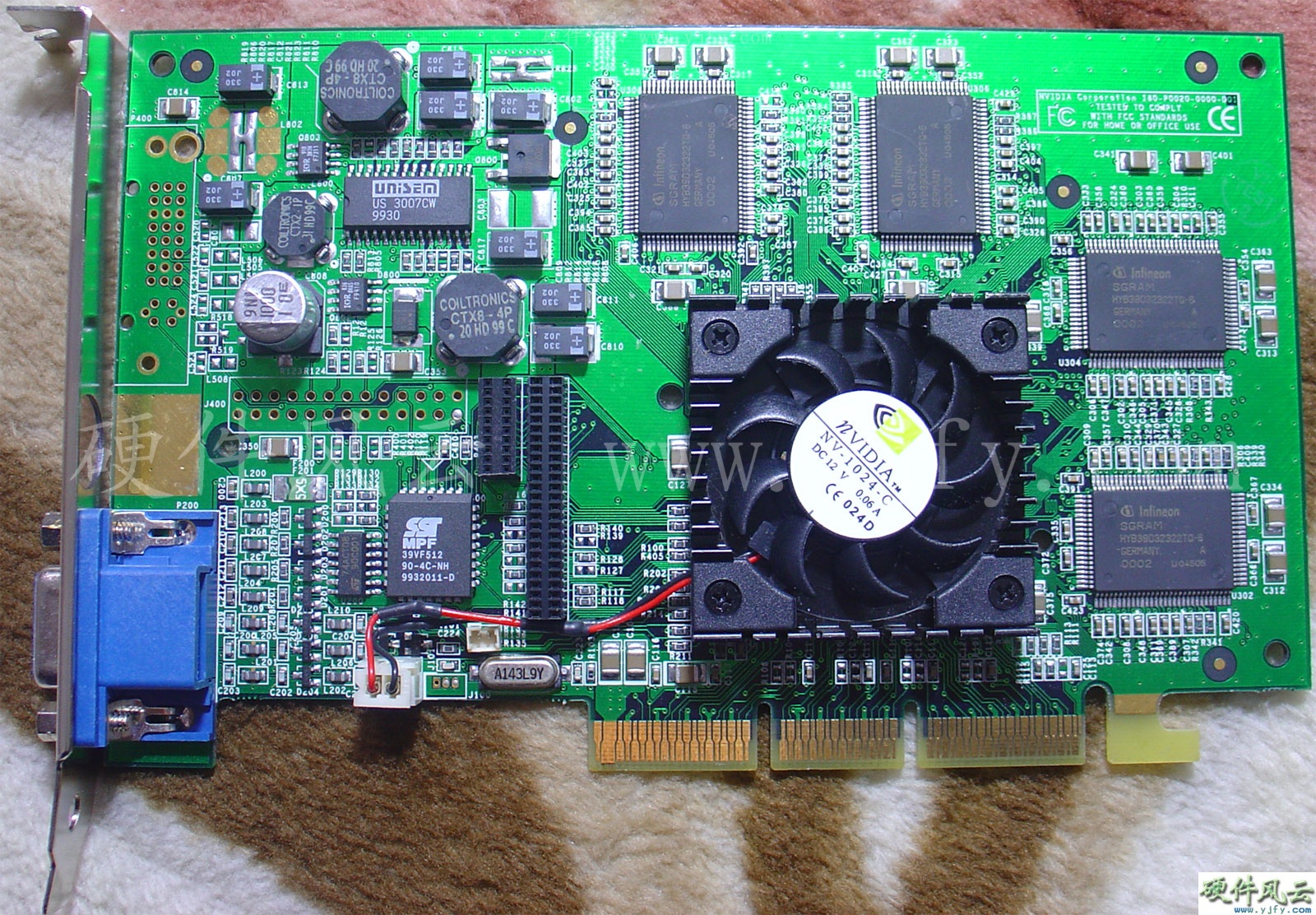
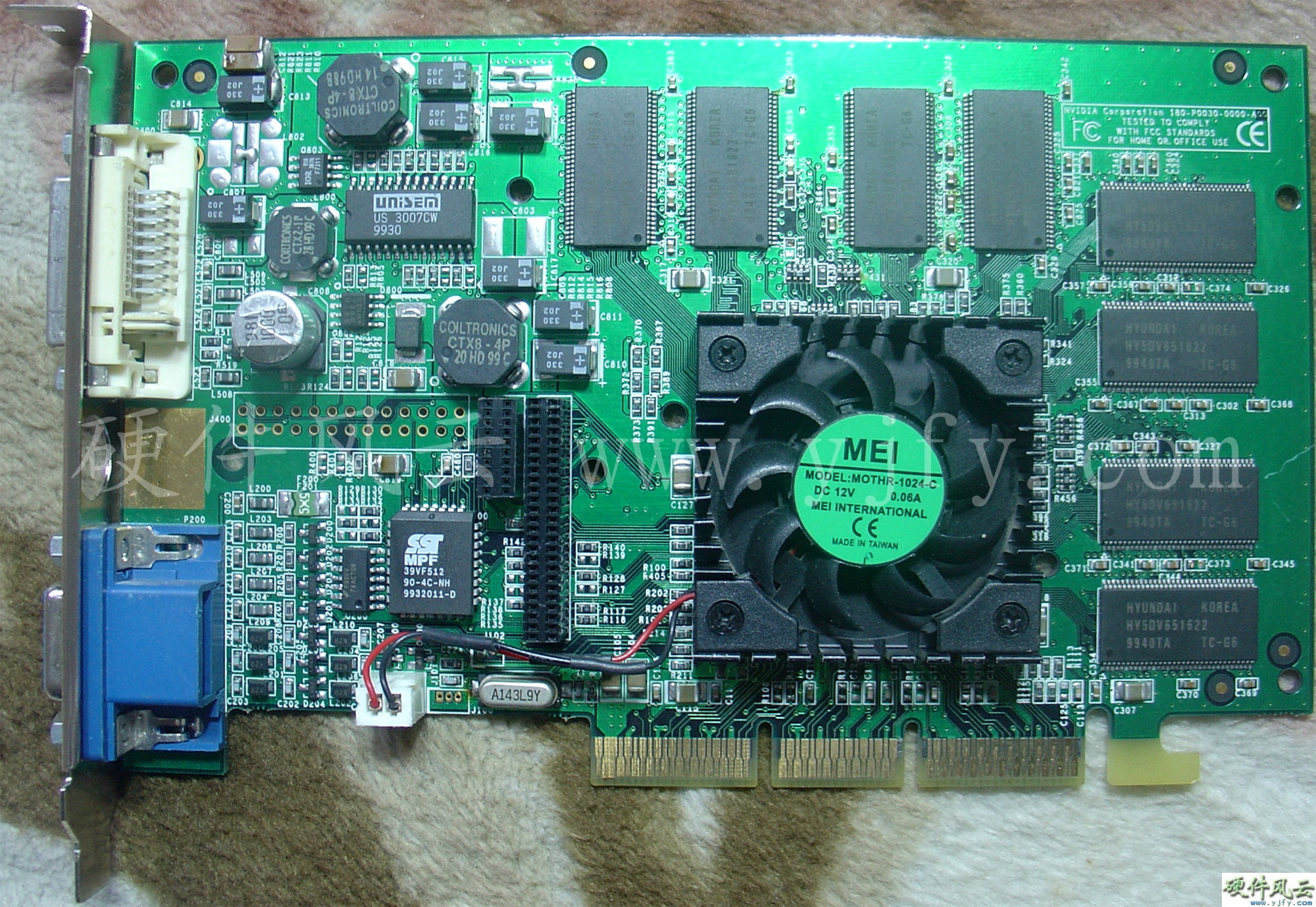
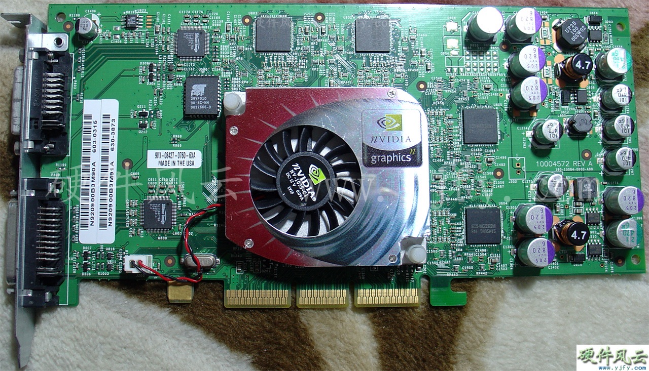
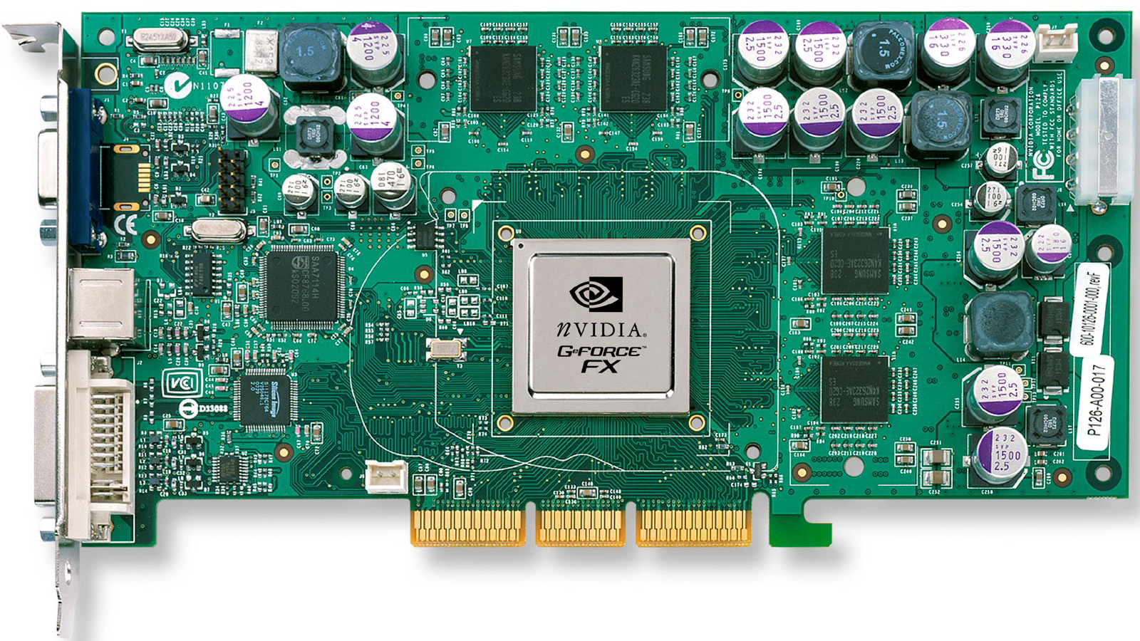
5.1.1.2 P126
Samsung developed the industry's first 1Gbps 128Mb GDDR2 SDRAM in July
2002. nVIDIA GeForce FX is the first graphics card to use GDDR2. On
November 18, 2002 (0247 week), COMDEX2002 released GeForce FX. The
promotional picture of GeForce FX at that time is the following picture.
The Samsung graphics memory particles on the engineering sample card of
the picture are the ES version and the date is 0238 weeks. The PCB date
should be 0240 or 0241 weeks.
GeForce FX5800 Ultra
Engineering sample
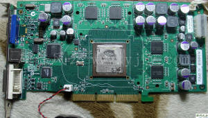
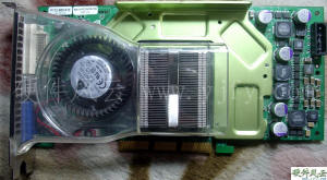
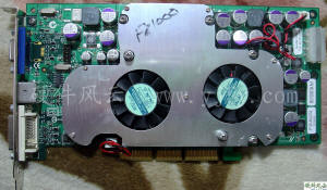
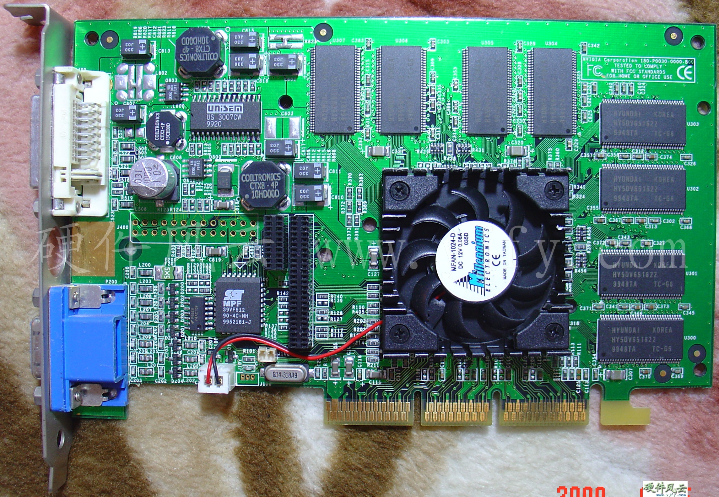
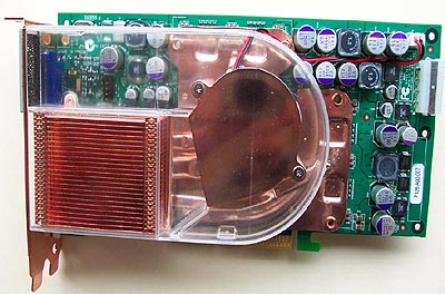
The GeForce FX of this
kind of turbo fan was also circulated on COMDEX 2002. It seems that the
design cost is slightly higher and was abandoned.
GeForce FX5800 Ultra
Engineering sample

(From
ixbtlabs.com)
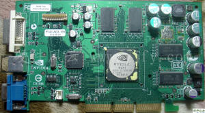
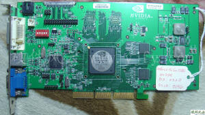
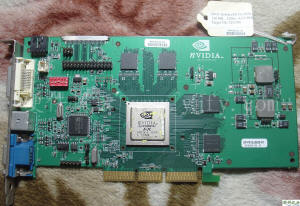
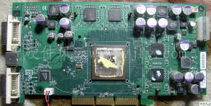
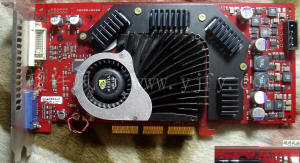
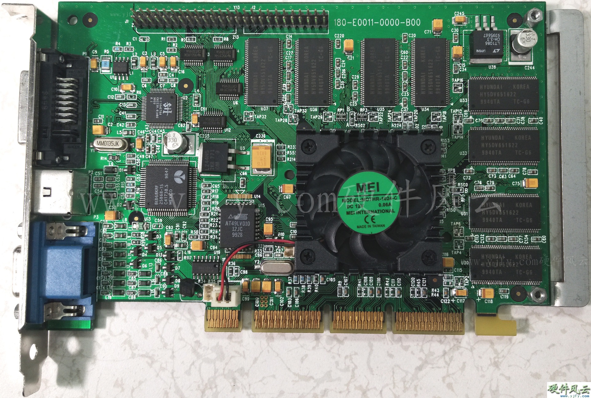
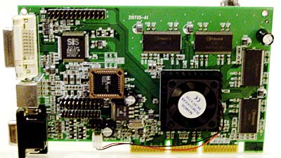
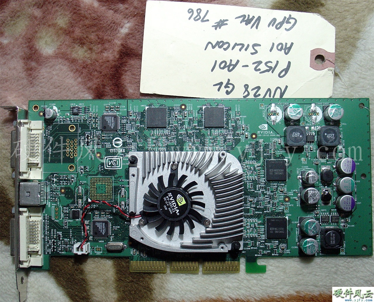
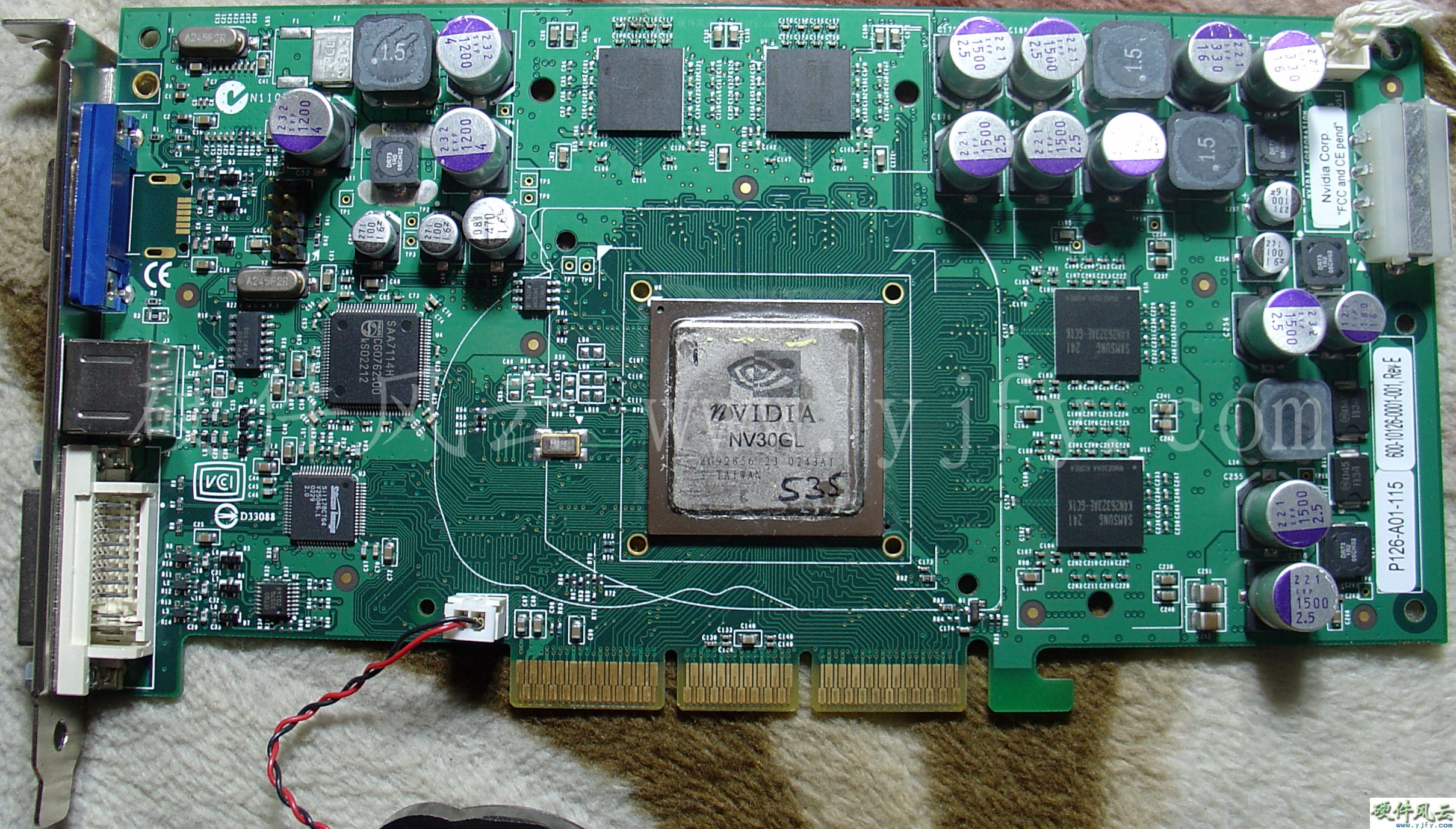
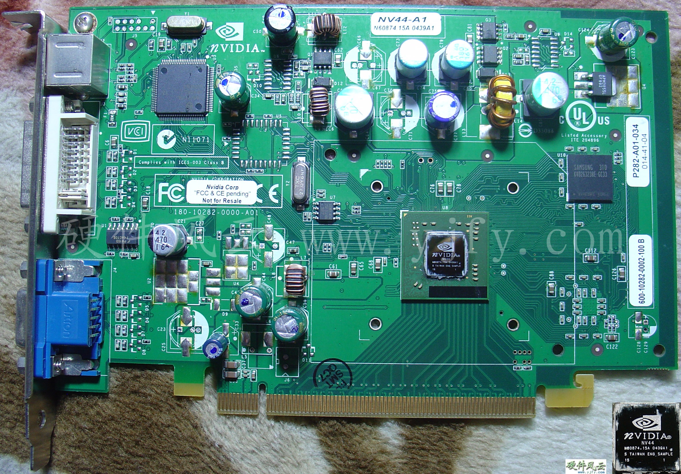
5.1.2 Rev A01
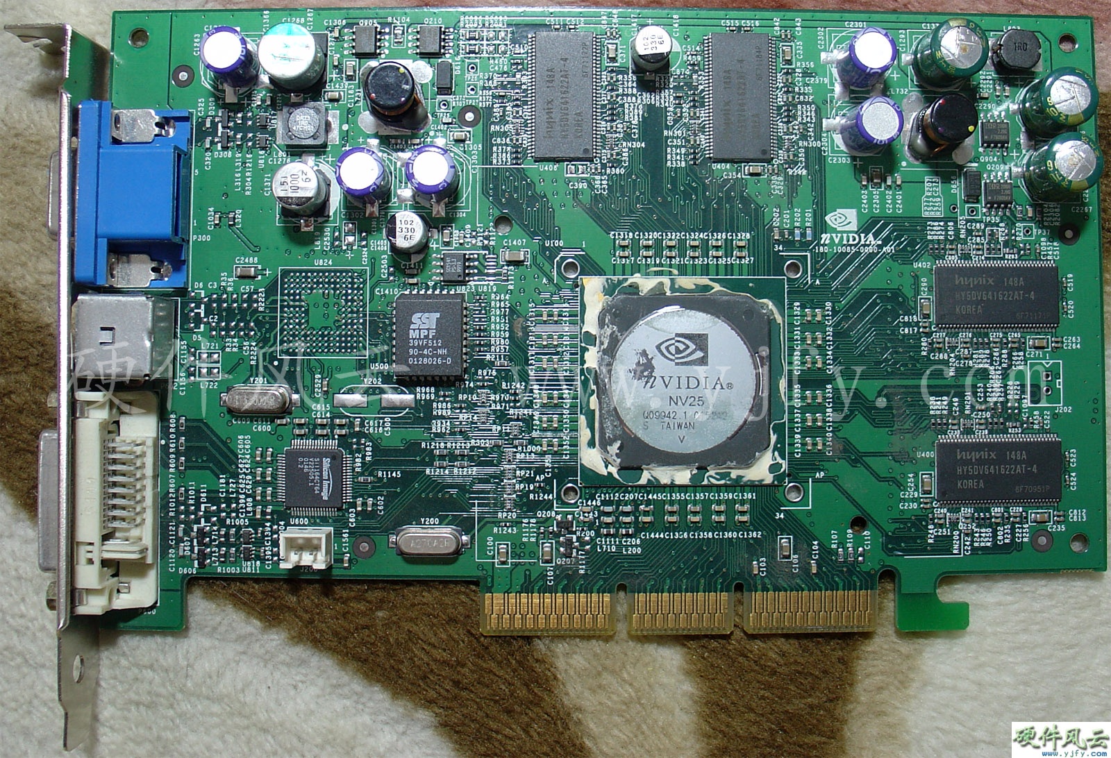
PCB Code:180-10126-0000-A01
Chip model:NV30GL A1
The video memory
particle date is 0241 weeks, which is the official version. The PCB date
is 0242 weeks, the NV30 chip date is 0243 weeks, and the version is A1.
Although the chip is marked as NV30GL, it is not distinguished as QUADRO
and GeForce FX. When the NV30 chip is the A2 version, it is marked as
GeForce FX to indicate formal mass production, and marked as QUADRO 2000
is still in the engineering sample stage.
This heat dissipation system is optional for GeForce FX. Due
to its low heat dissipation capacity, it is mainly used for the heat
dissipation of low-end graphics cards.
GeForce FX5800 Ultra
Engineering sample
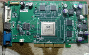
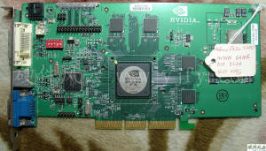
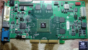
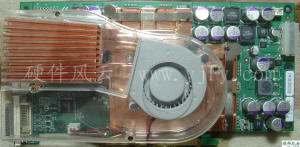
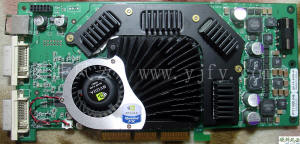
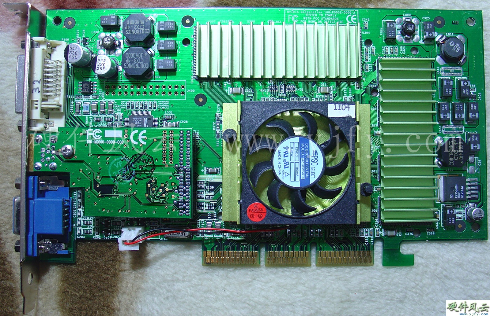
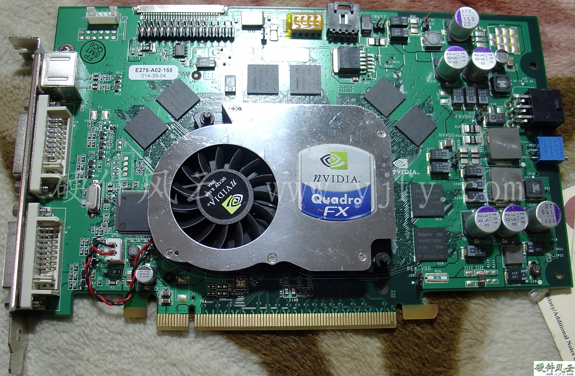
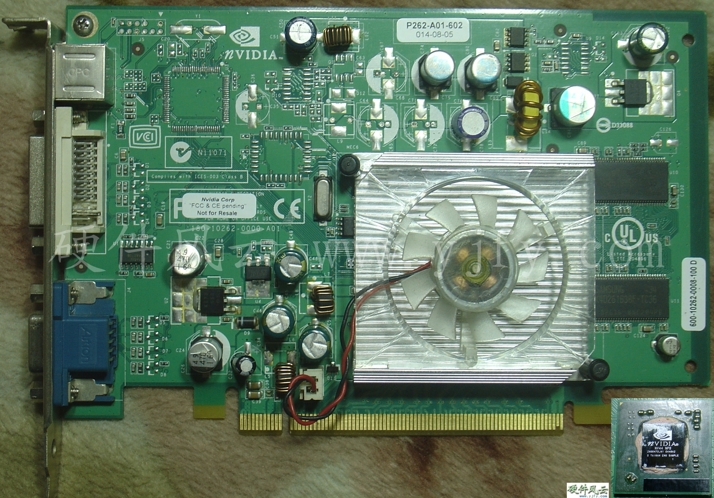
5.1.3 Rev A02
PCB Code:180-10126-0000-A02
Chip model:NV30GL A1
The
chip date is 0244 weeks, and the PCB date is 0244 weeks.
This slightly lower cost turbo radiator (nVIDIA's FX Flow
cooling technology) was selected and finally adopted.
GeForce FX5800 Ultra
Engineering sample
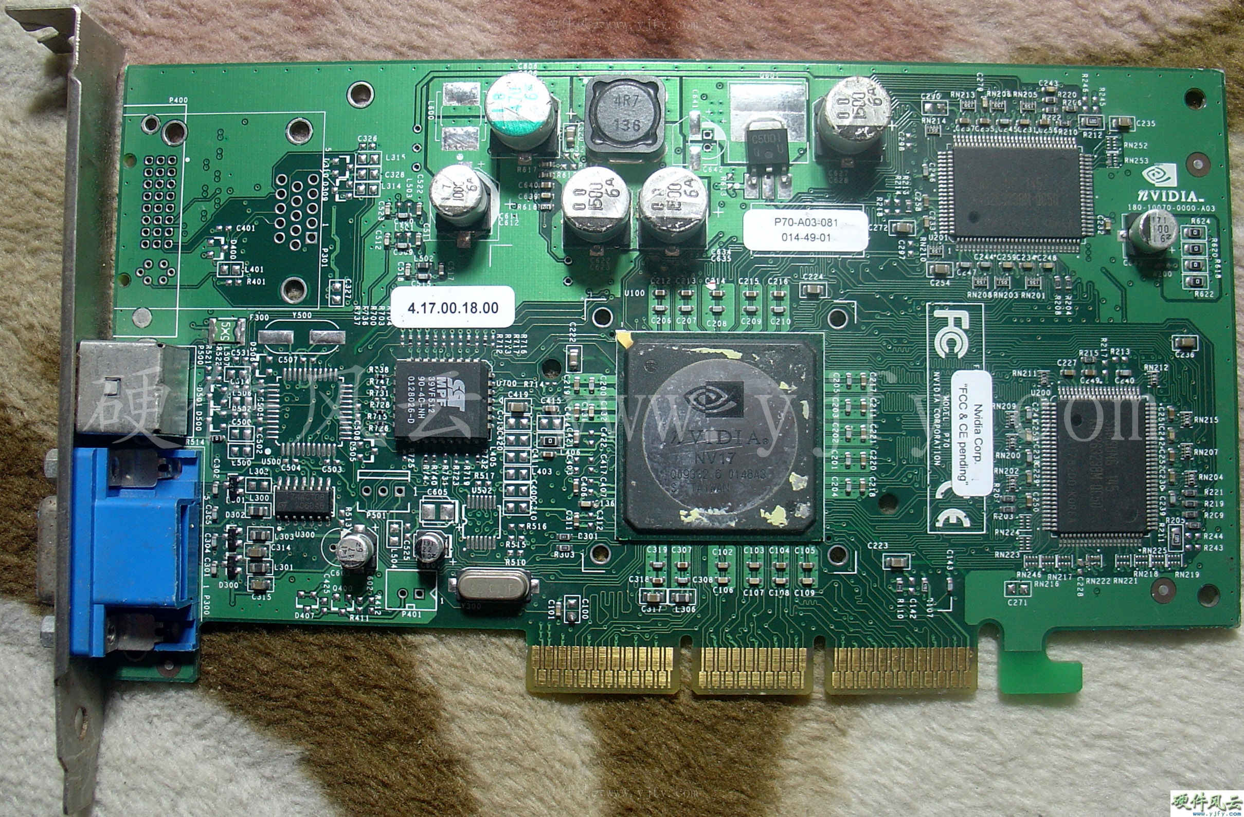
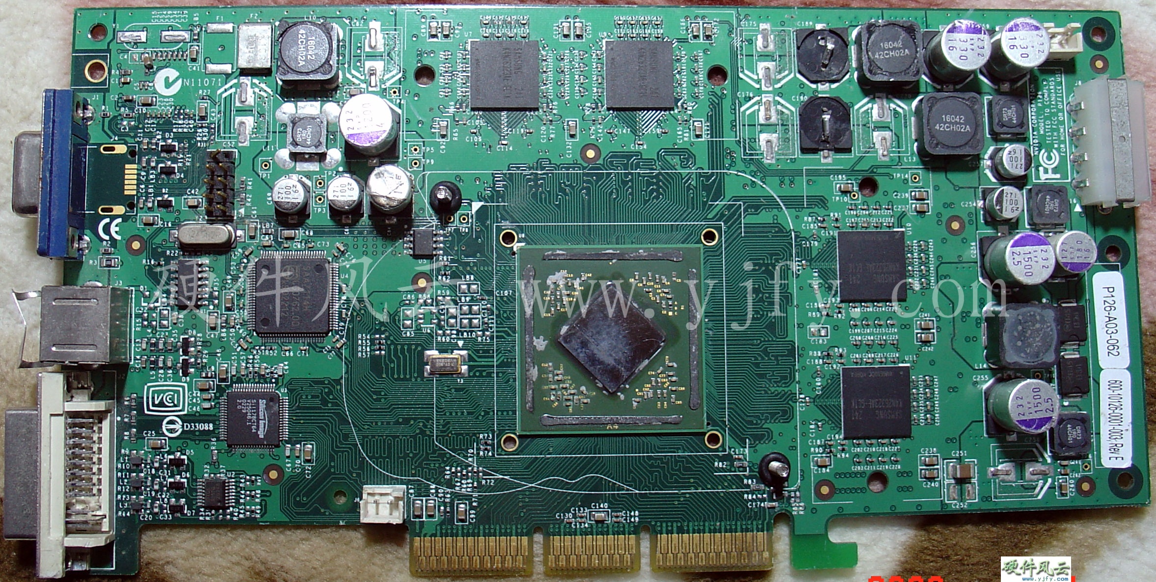
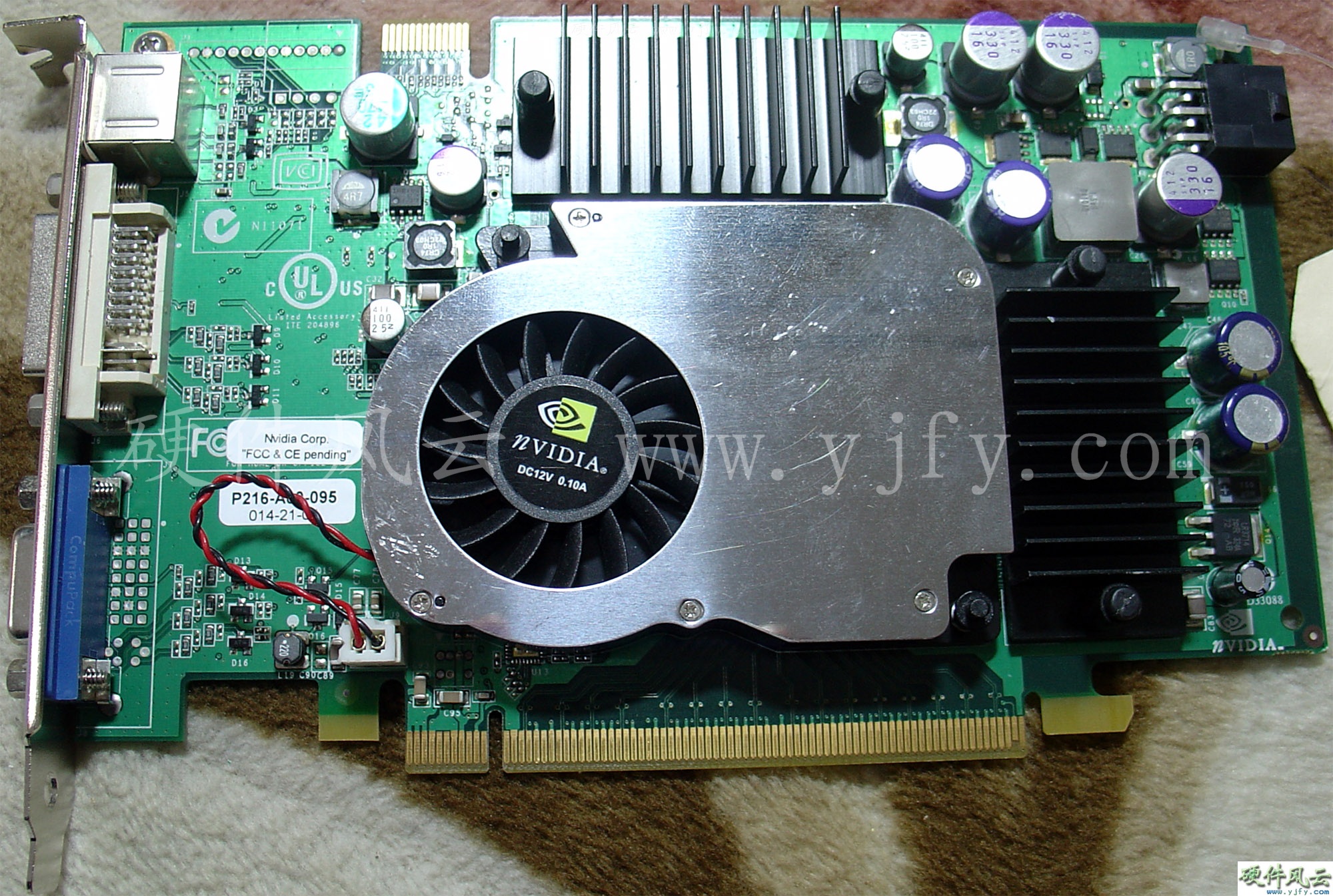
5.1.4 Rev A03
PCB Code:180-10126-0000-A03
PCB date is 0245 weeks.
GeForce FX5800 Ultra
Engineering sample

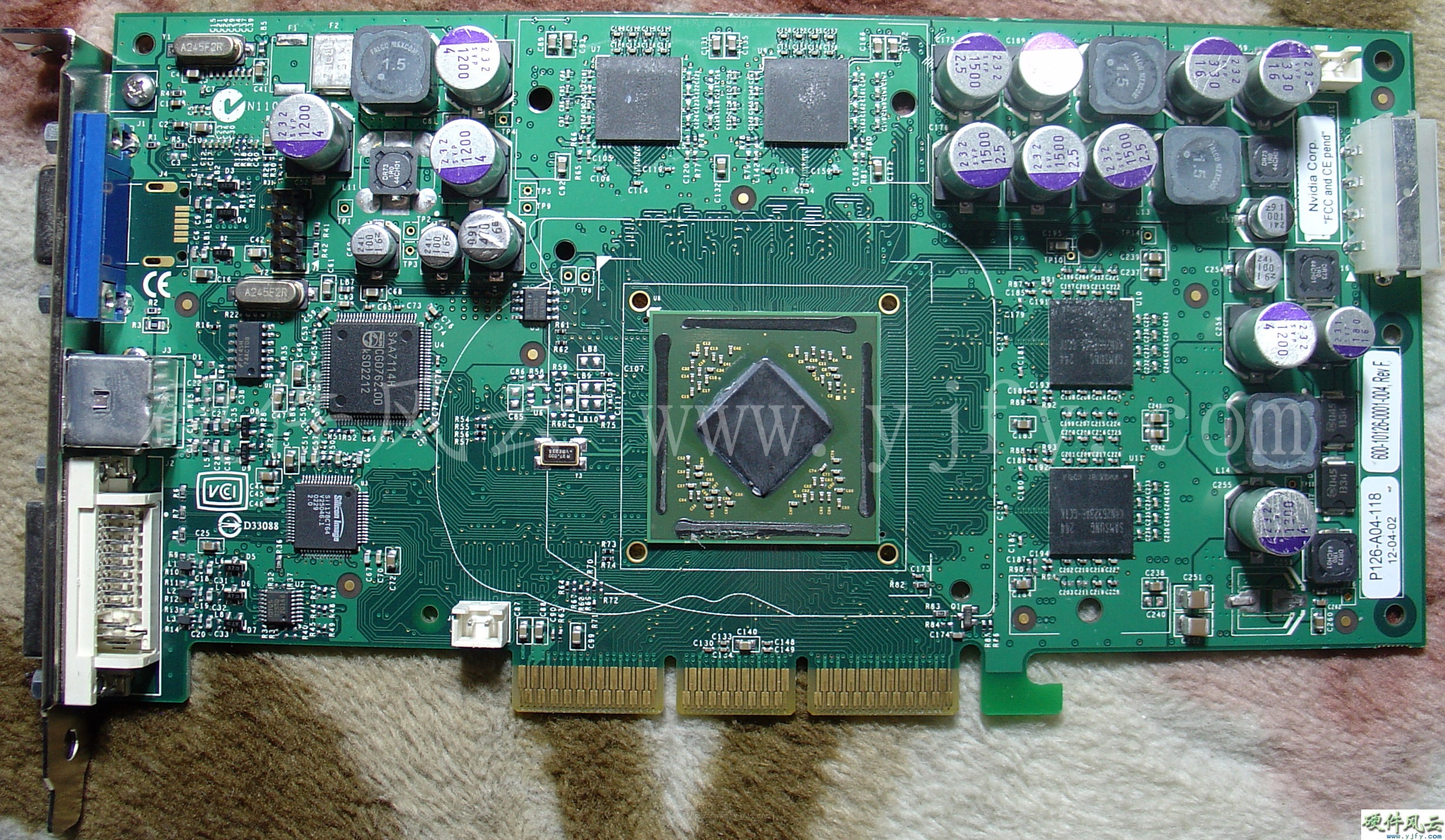
5.1.5 Rev A04
PCB Code:180-10126-0000-A04
PCB date is 0249 weeks.
GeForce FX5800 Ultra
Engineering sample

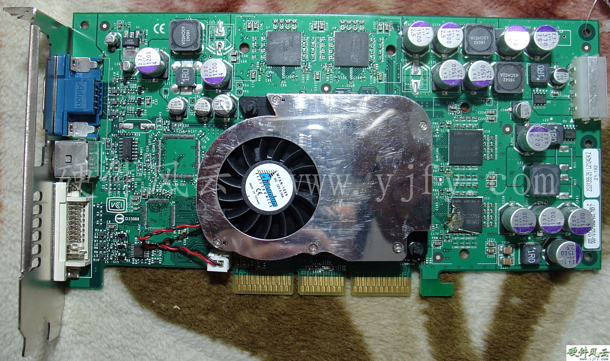
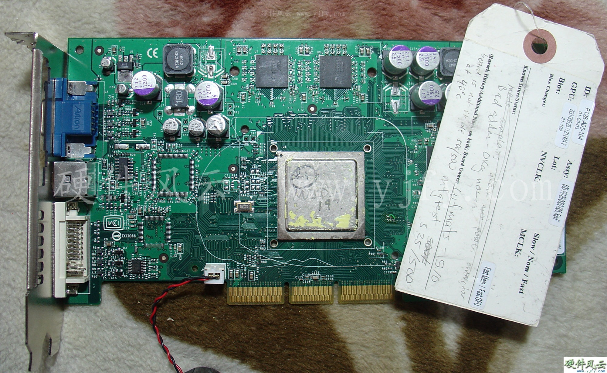
5.1.6 Rev A05
PCB Code:180-10126-0000-A05
PCB date is 0251 weeks.
This revised version has been revised and
officially finalized. This card is still undergoing important tests on
GDDR2 video memory and even the chip. It can be seen that until the
final GeForce FX5800 Ultra is finalized, there are still many problems
in the hardware, but time is not waiting, so we can only bet on the
driver. The final engineering sample PCB date is 0301 weeks.
GeForce FX5800 Ultra
Engineering sample


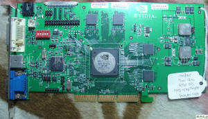
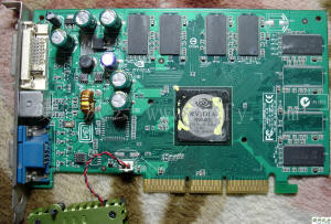
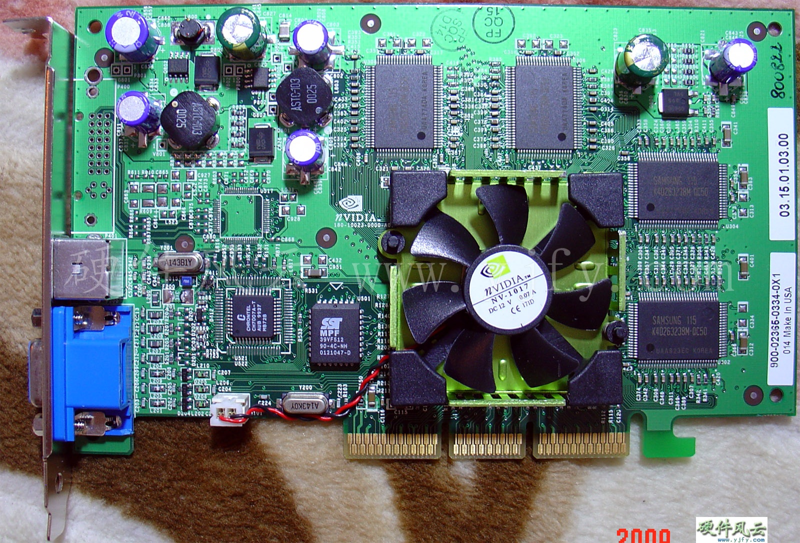
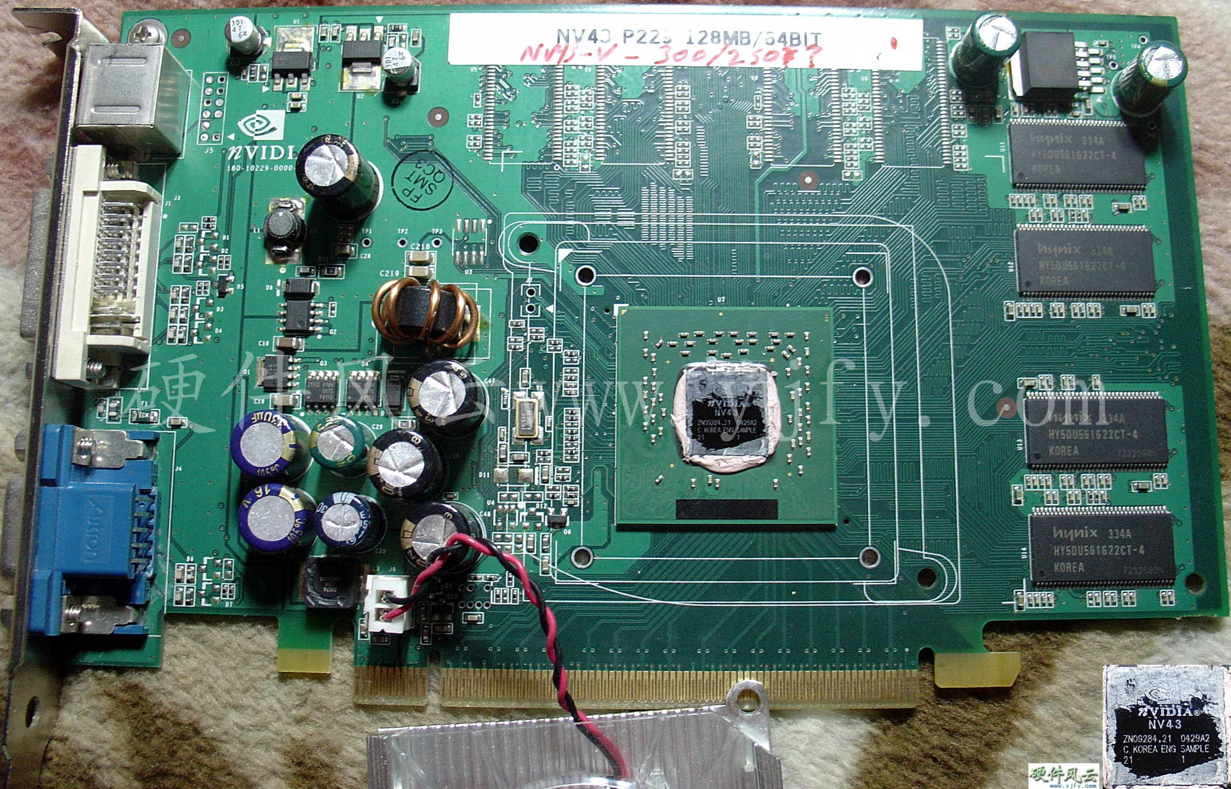
5.2
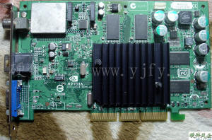
GeForce FX5200/FX5200 Ultra
Released on March 6, 2003.
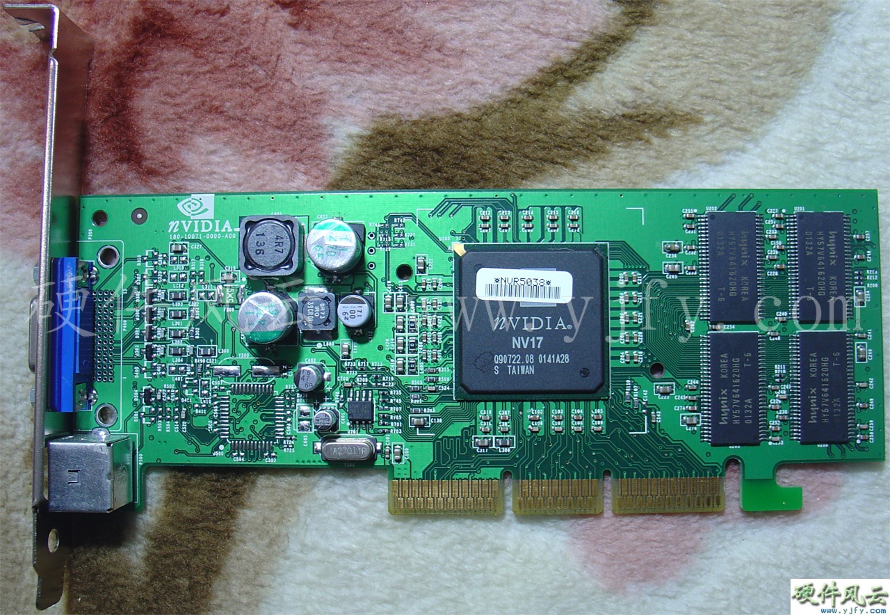
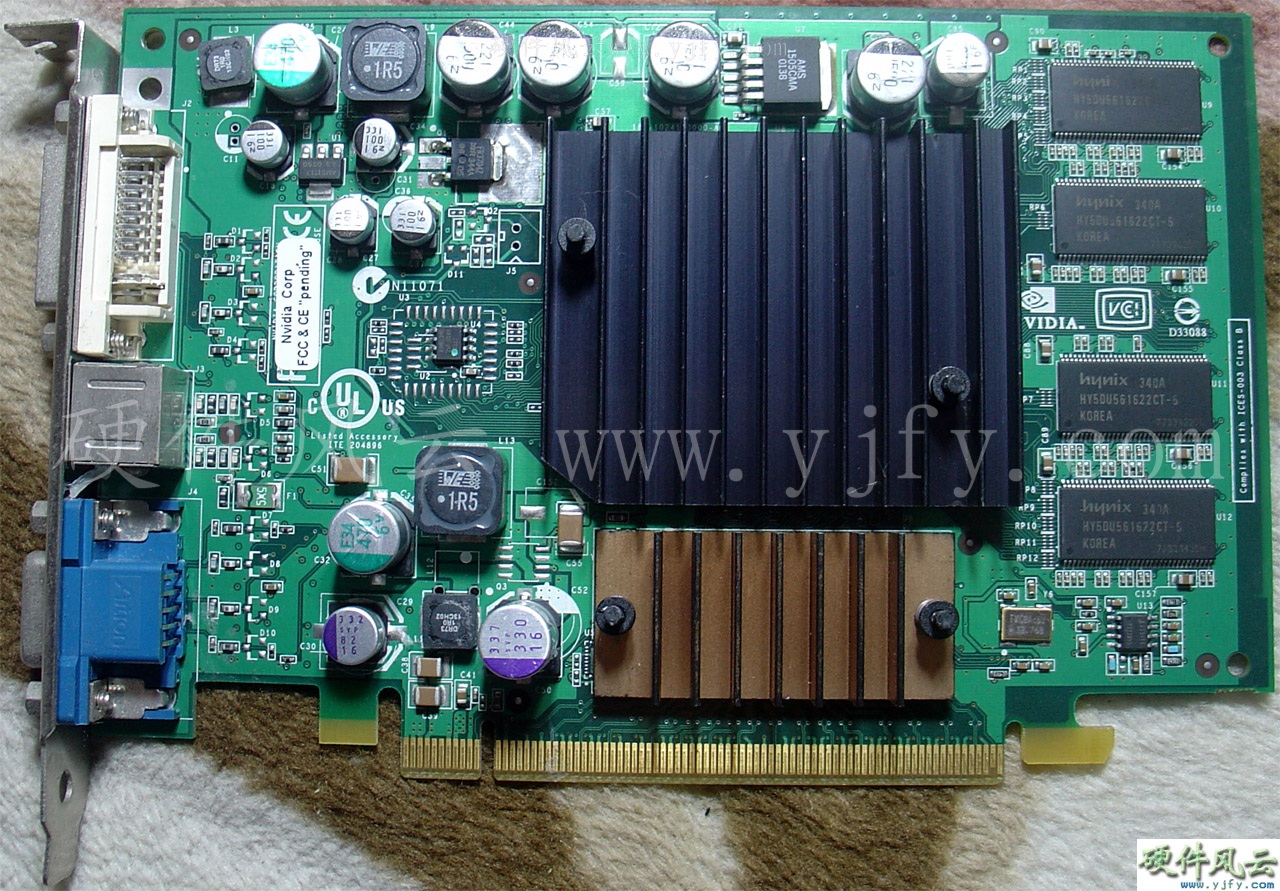
5.2.1 E133
PCB Code:180-10133-0000-A01
Chip model:NV34 A1B2
ES
Chip date is 0303 weeks, PCB date is 0305 weeks.
GeForce FX5200 Engineering sample
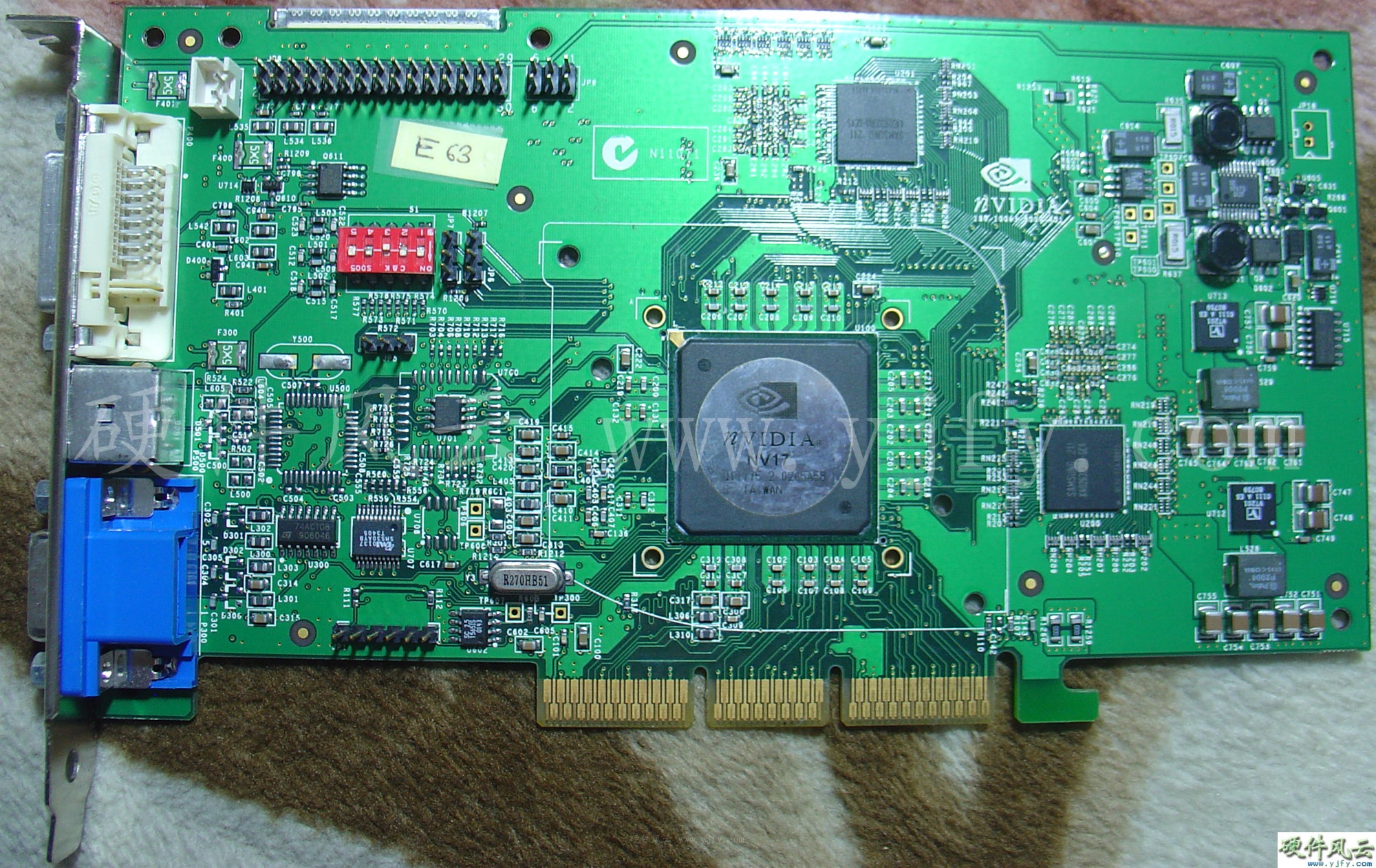
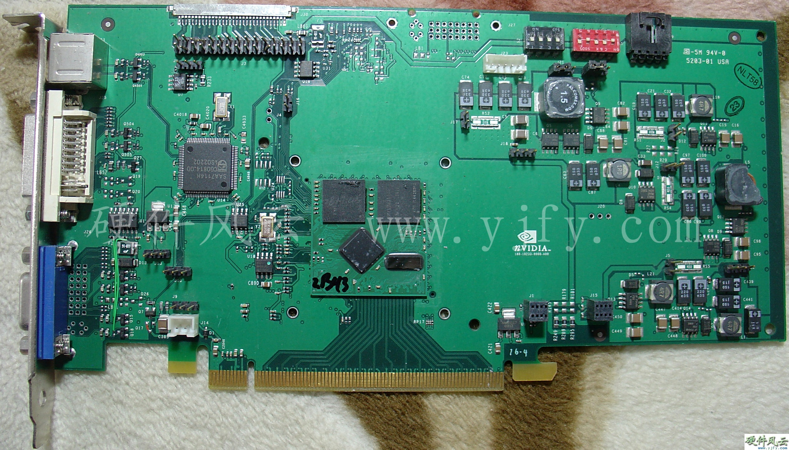
5.2.2 P162
Chip model:NV34-A2
PCB Code:180-10162-0000-A03
Chip date is 0309 weeks, PCB date is 0309 weeks.
GeForce FX5200 Engineering sample
5.2.3 P140
PCB Code:180-10140-0000-A01
Chip model:NV34U A2
Chip date is 0309
weeks, PCB date is 0309 weeks.
GeForce FX5200 Ultra Engineering sample
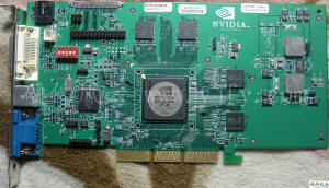
5.3
GeForce FX5600/FX5600 Ultra
Released on March 6, 2003.
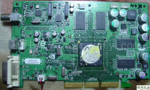
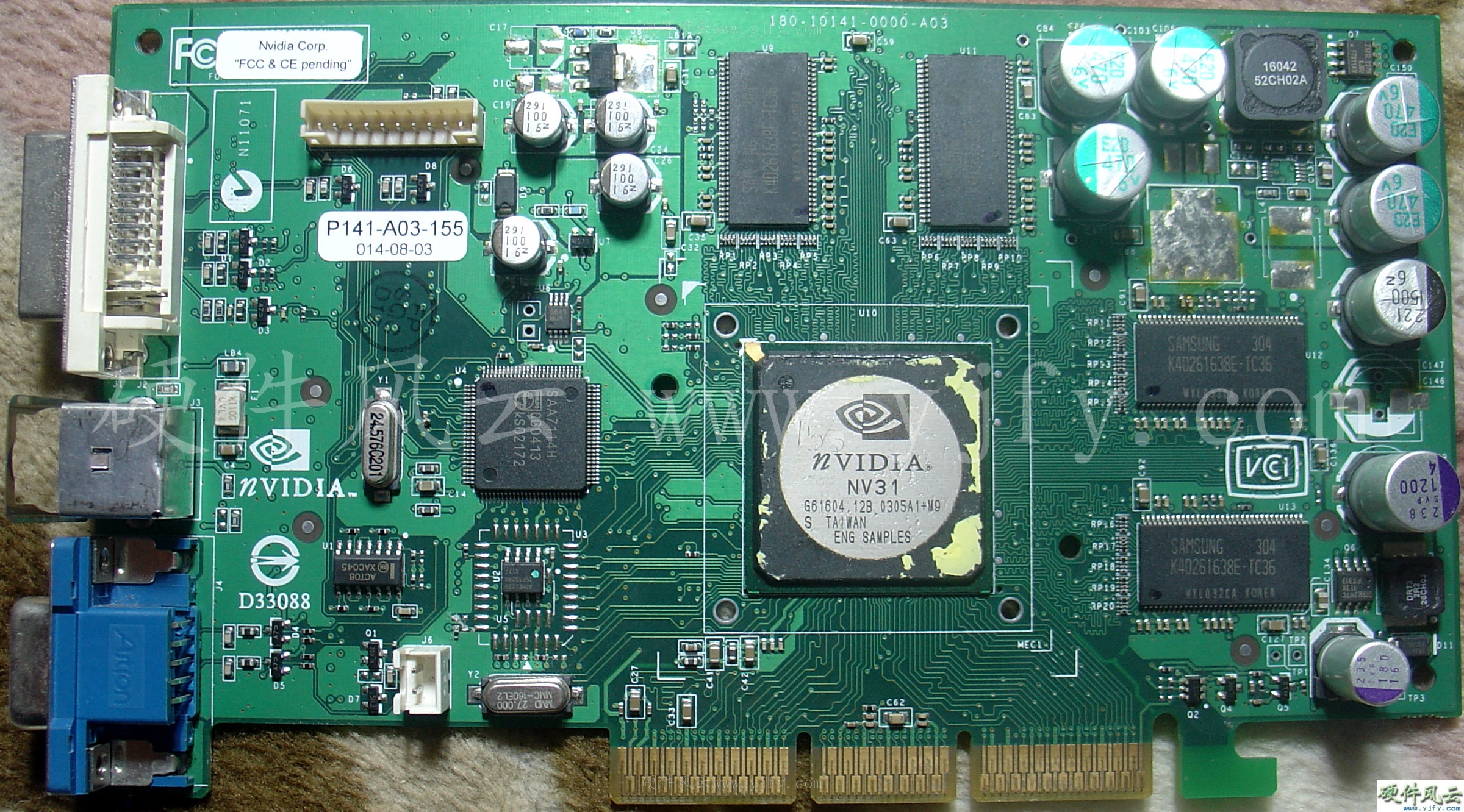
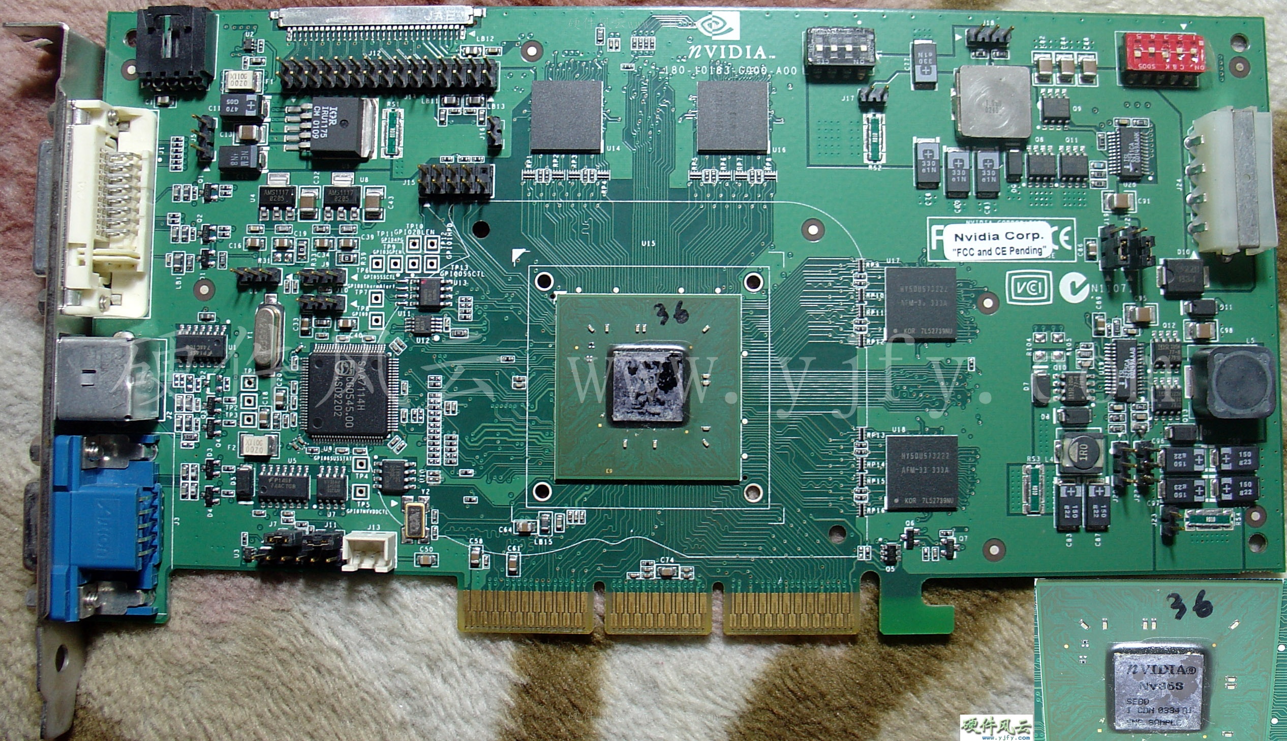
5.3.1 P141
PCB Code:180-10141-0000-A01
Chip model:NV31 A1+M9 ES
Chip date is 0305 weeks, PCB date is 0309 weeks.
GeForce FX5600
Engineering sample
5.3.2 P140
Chip model:NV31FC
A1 ES
PCB Code:180-10140-0000-A01
Chip date is 0318 weeks, PCB date is 0320 weeks.
GeForce FX5600 Ultra
Engineering sample
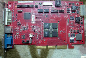
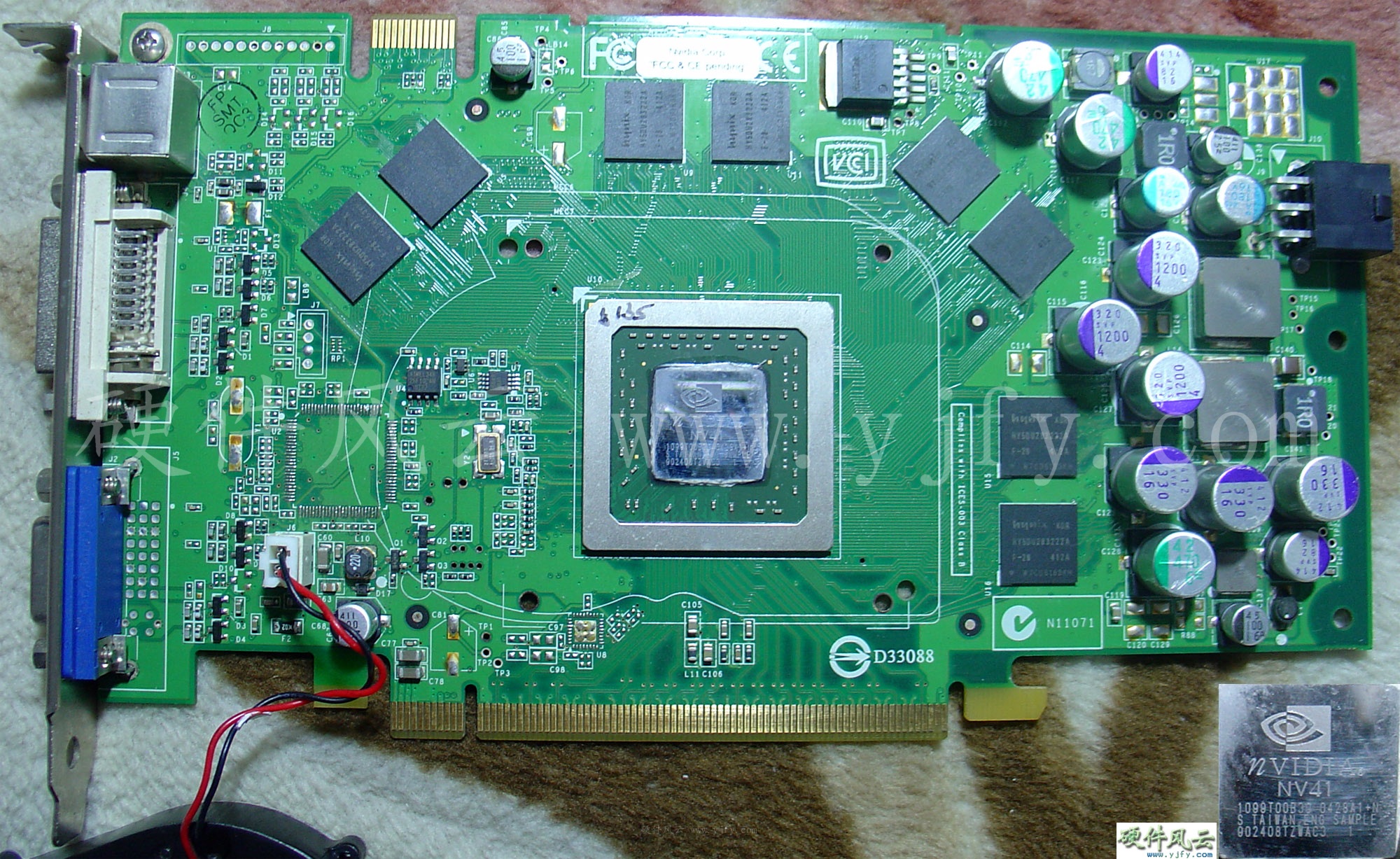
5.4
GeForce FX5700/FX5700 Ultra
Released on October 23, 2003.
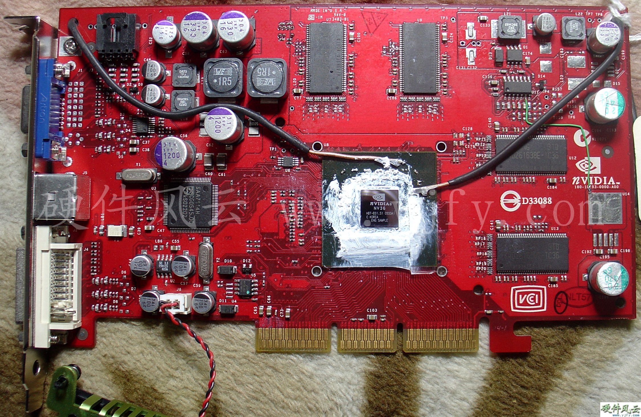
5.4.1 P193
Chip model:NV36 A1 ES
PCB Code:180-10193-0000-A00
Chip date is 0333 weeks, PCB date is 0334 weeks. Most of nVIDIA's PCBs
are green, and red ones are very rare.
GeForce FX5700 Engineering sample

5.4.2 E183
Chip model:NV36S A1
ES
PCB Code:180-10183-0000-A00
Chip date is 0334 weeks, PCB date is 0330 weeks.
GeForce FX5700
Engineering sample
5.4.3 P190
PCB Code:180-10190-0000-A03
Chip model:GF-FX-5700-U-A1
Chip date is 0346 weeks, PCB date is 0342 weeks.
GeForce FX5700 Ultra
Engineering sample
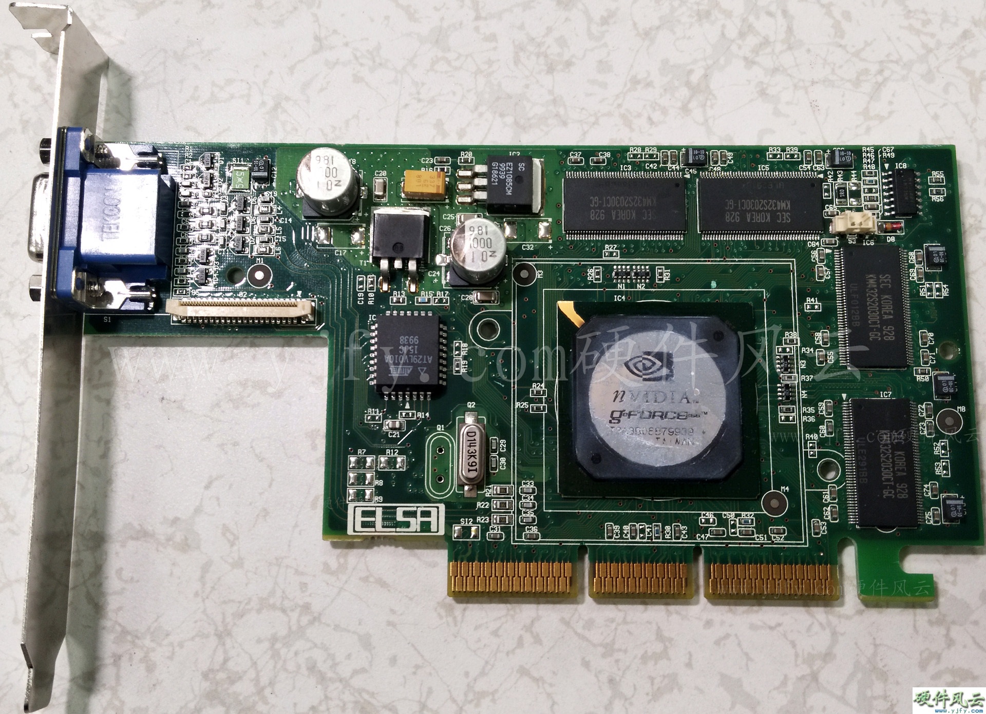
5.5
GeForce FX5900/FX5900 Ultra
2003年5月12日发布。
5.5.1 P172-A00
Chip model:NV35 A1
PCB Code:180-10172-0000-A00
Chip date is 0310 weeks.
GeForce FX5900
Engineering sample
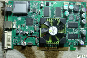
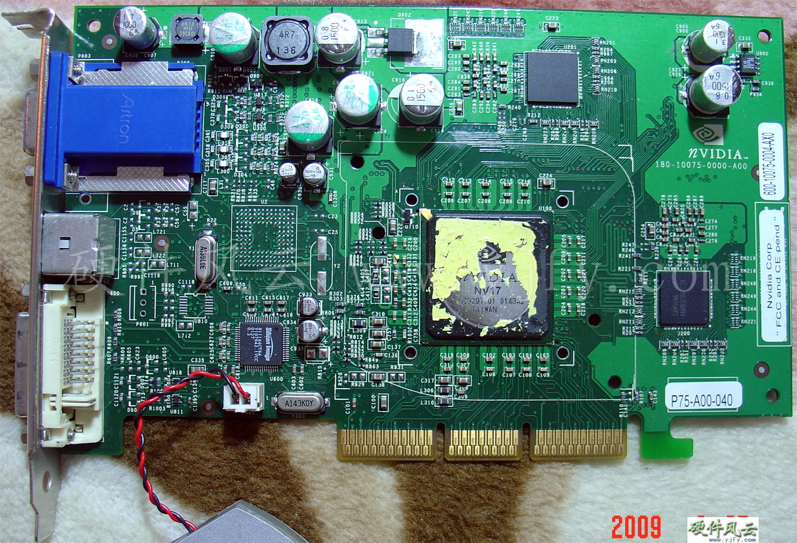
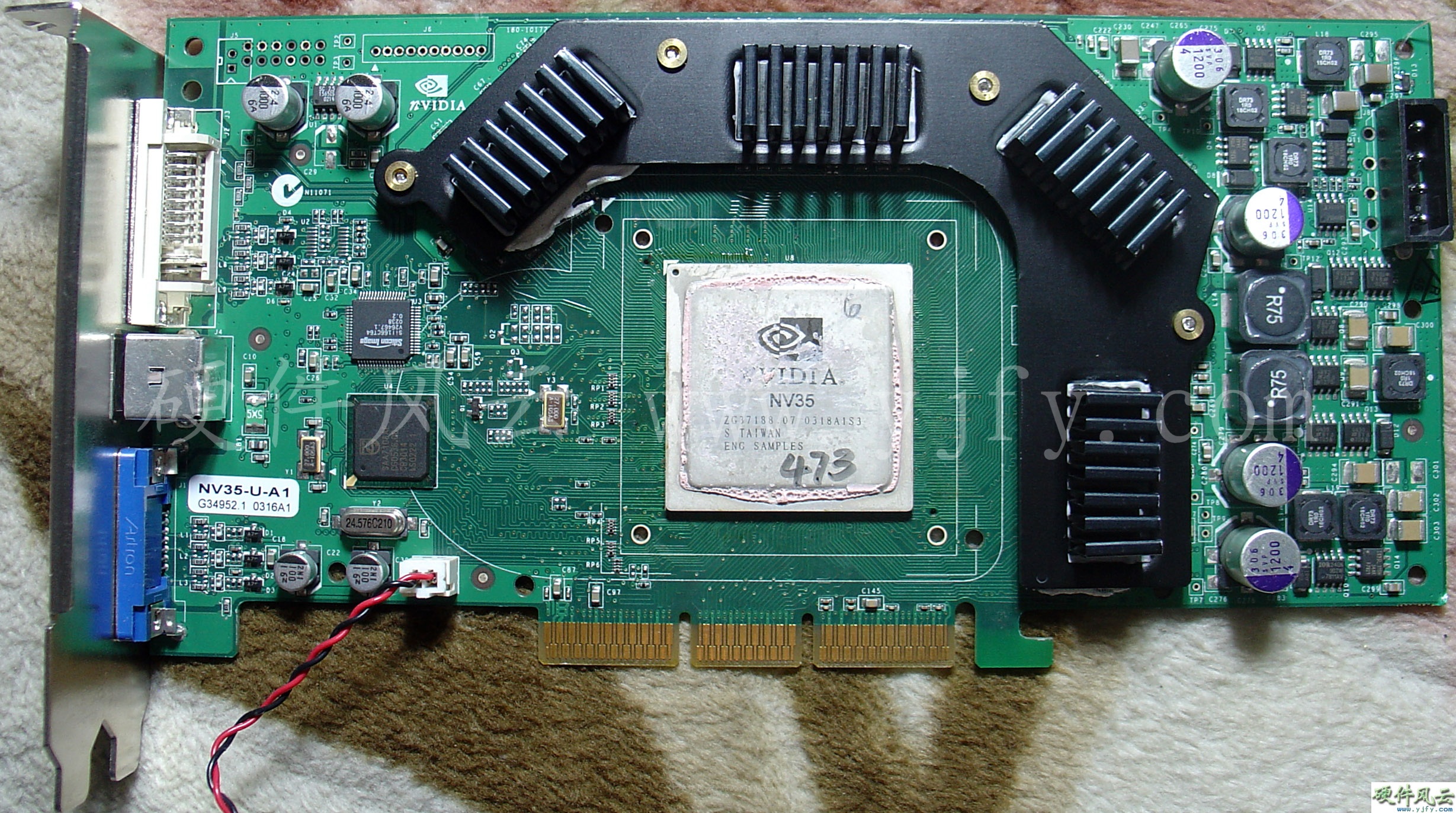
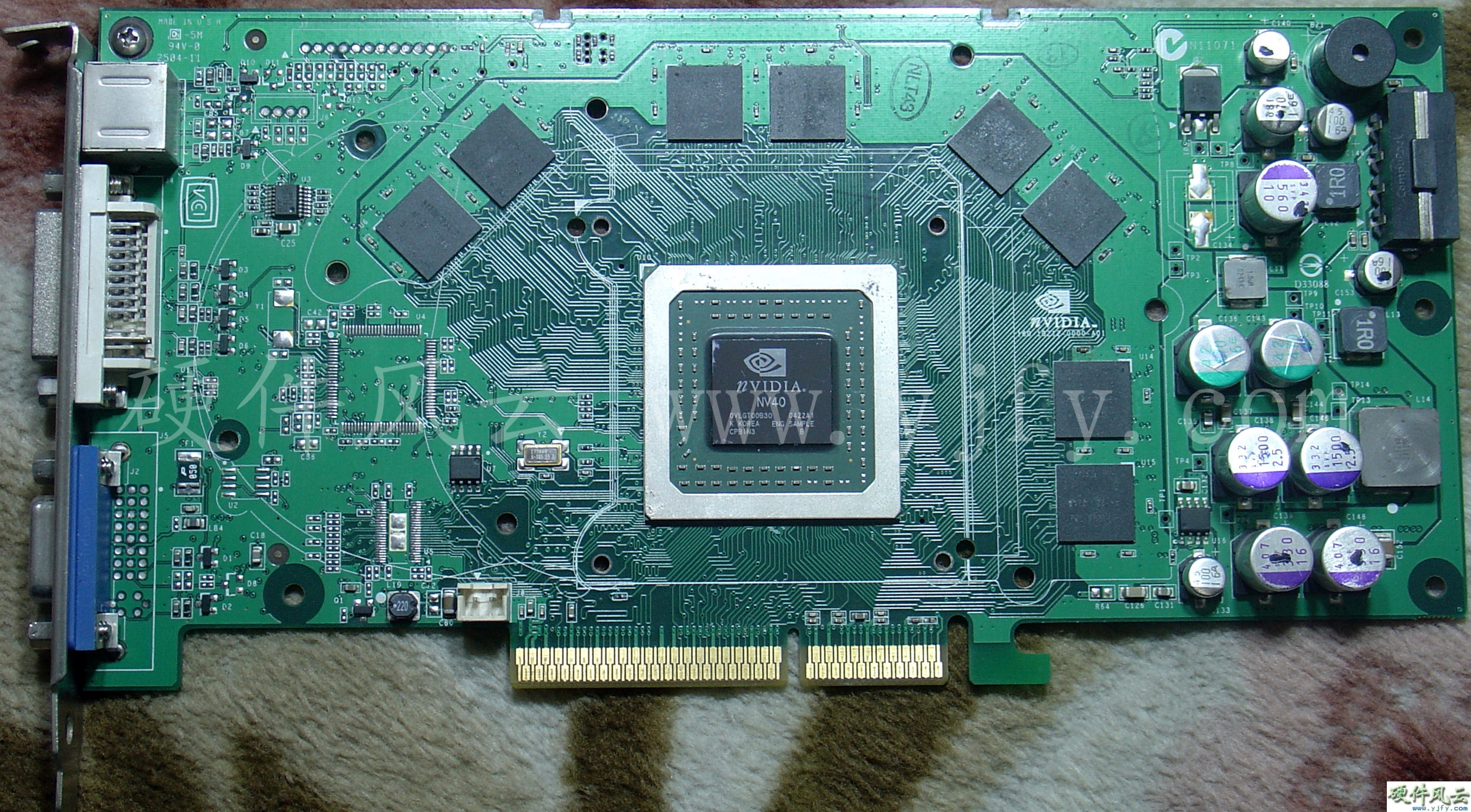
5.5.2 P172-B00
Chip model:NV35-U-A1 ES
PCB Code:180-10172-0000-B00
Chip date is 0329 weeks, PCB date is 0335 weeks.
GeForce FX5900 Ultra
Engineering sample

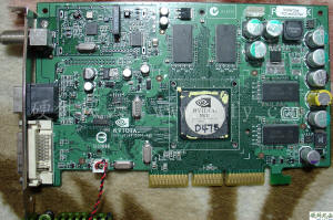
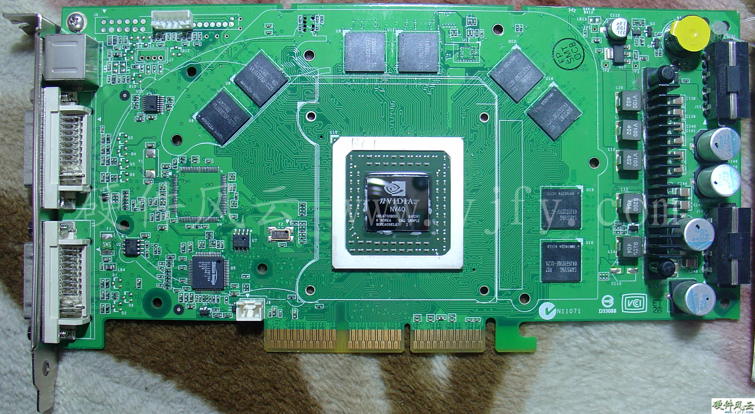
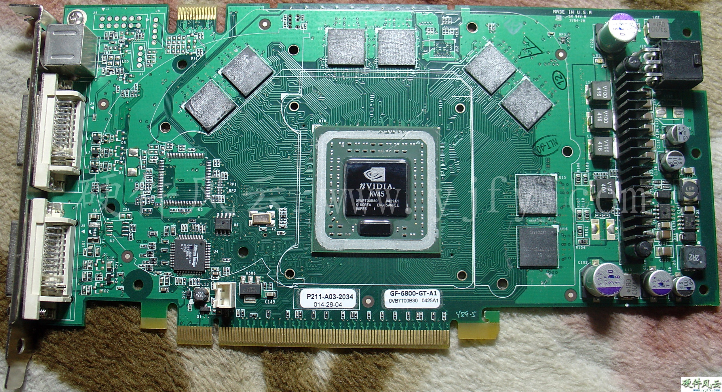
5.6 GeForce FX5950
Ultra
On October 23, 2003, nVIDIA released the GeForce FX5950 Ultra.
Model:P172-B00
Chip model:FX5900U-A1
PCB Code:180-10172-0000-B00
Chip date is 0329 weeks, PCB date is 0333 weeks.
GeForce FX5950 UltraEngineering
sample

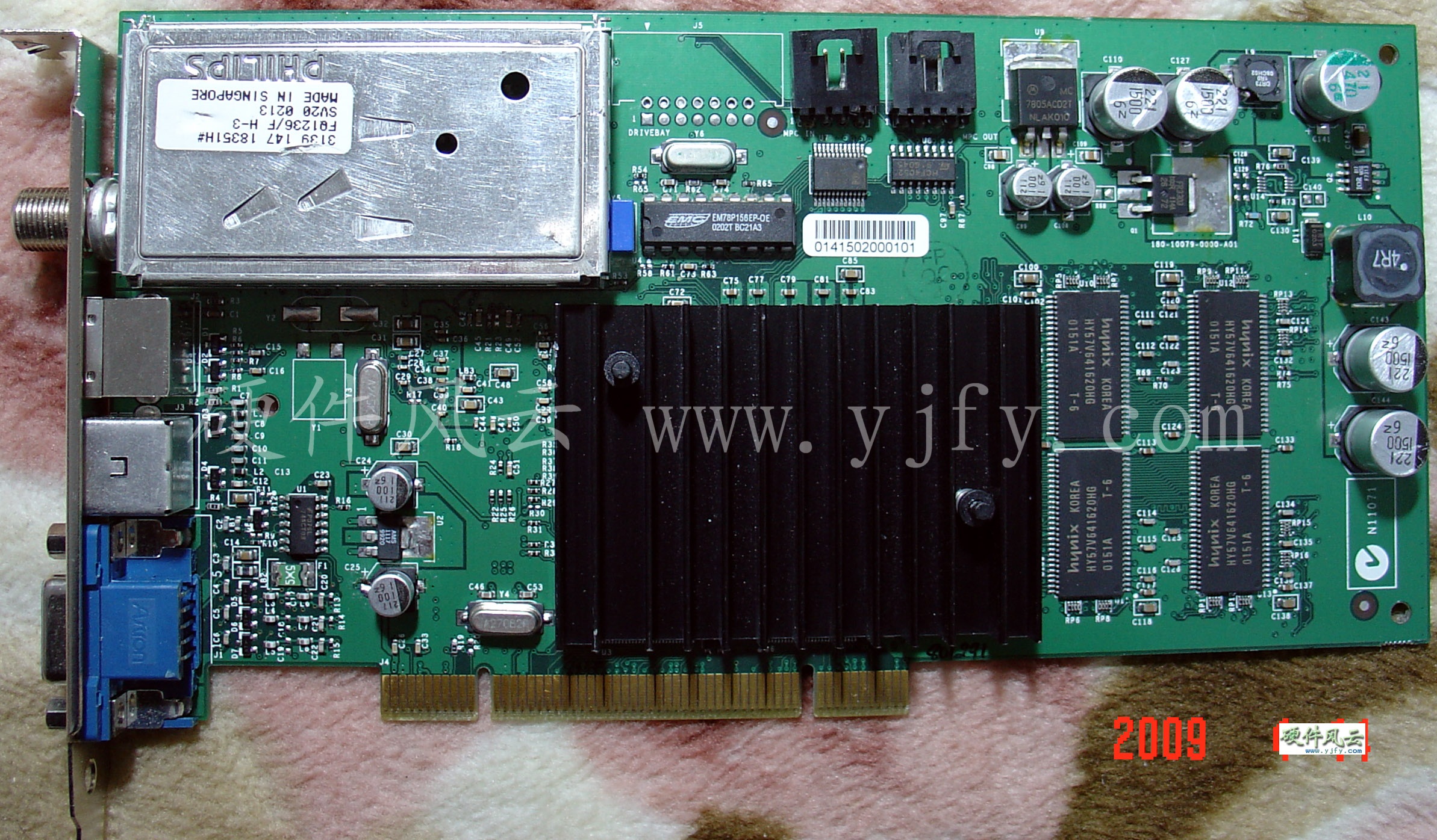
5.7 Personal cinema
FX5200
5.7.1 P143
PCB Code:180-10143-0000-B01
Chip model:FX5200 A2
Chip date is 0318 weeks, PCB date is 0341 weeks.
Personal cinema
FX5200
Engineering sample
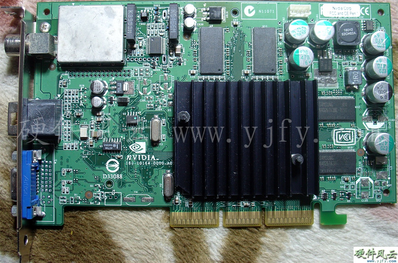
5.7.2 P164
PCB Code:180-10164-0000-A01
Chip model:NV34 A2 ES
The chip date is 0308
weeks, and the PCB date is 0306 weeks.
Personal cinema
FX5200
Engineering sample
5.8 Personal cinema
FX5600
5.8.1 P143 A00
Chip model:NV31 A1+9
ES
PCB Code:180-10143-0000-A00
Chip date is 0310 weeks, PCB date is 0309 weeks.
Personal cinema FX5600 Engineering sample
5.8.2 P143 B00
Chip model:FX5600 A1
PCB Code:180-10143-0000-B00
Chip date is 0321
weeks, PCB date is 0306 weeks.
Personal cinema FX5600 Engineering sample
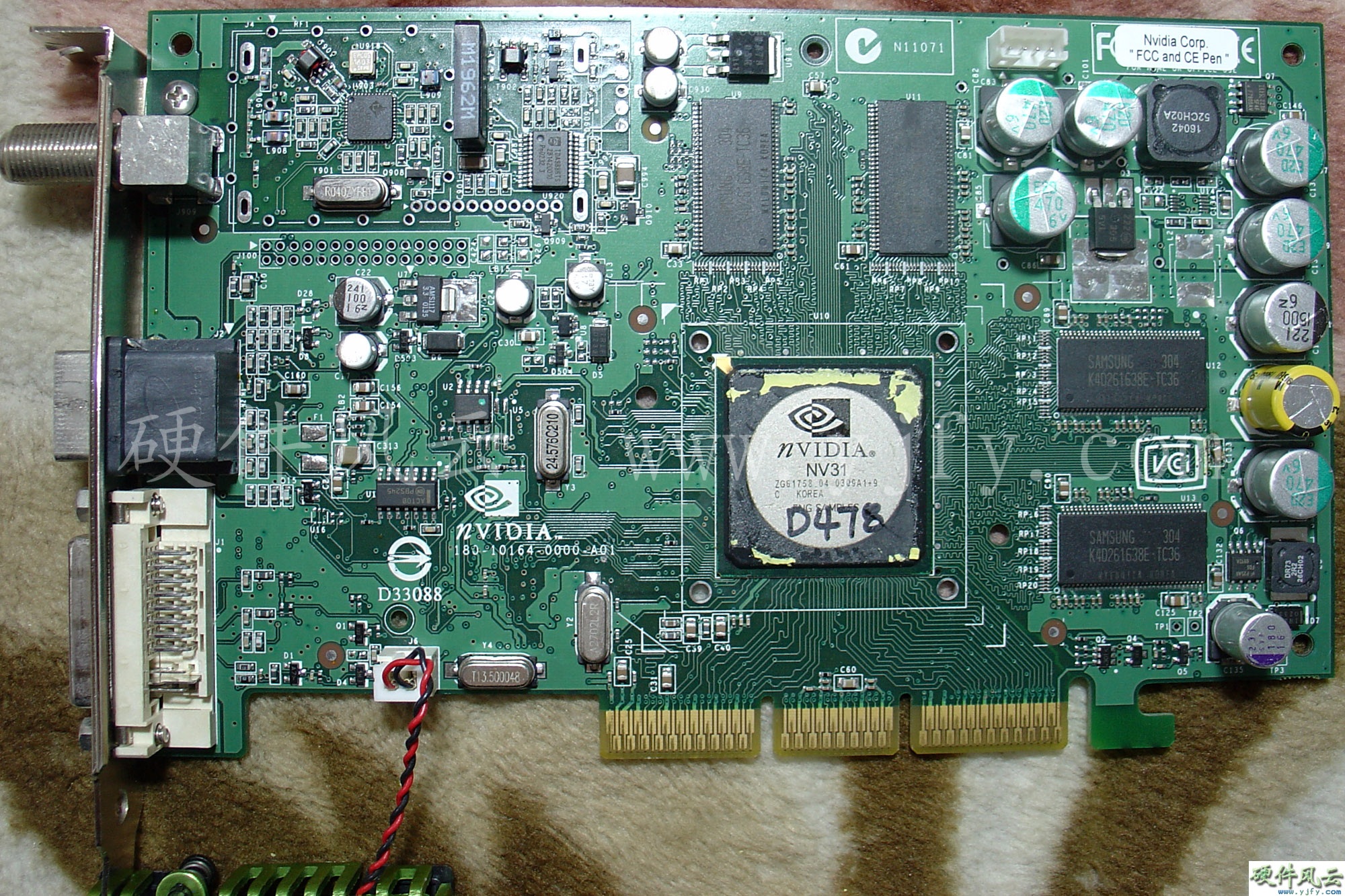
5.8.3 P164
PCB Code:180-10164-0000-A01
Chip model:NV31 A1+9
ES
Chip date is 0310 weeks, PCB date is 0327 weeks.
Personal cinema
FX5600
Engineering sample
5.9 Personal cinema
FX5700
Model:P178
PCB Code:180-10178-0000-A02
Chip model:FX5700 A1
Chip date is 0403 weeks, PCB date is 0404 weeks.
Personal cinema
FX5700
Engineering sample

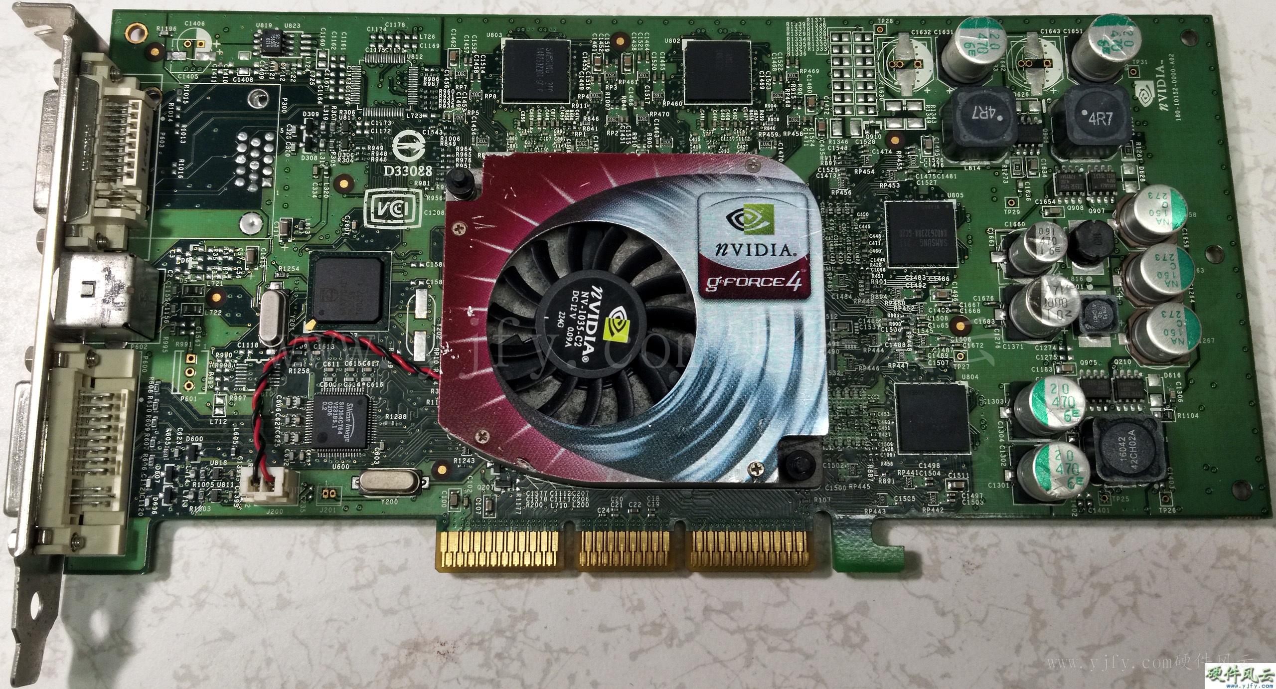
And Personal Cinema FX5900 is a GeForce FX5900
graphics card equipped with a video daughter card.
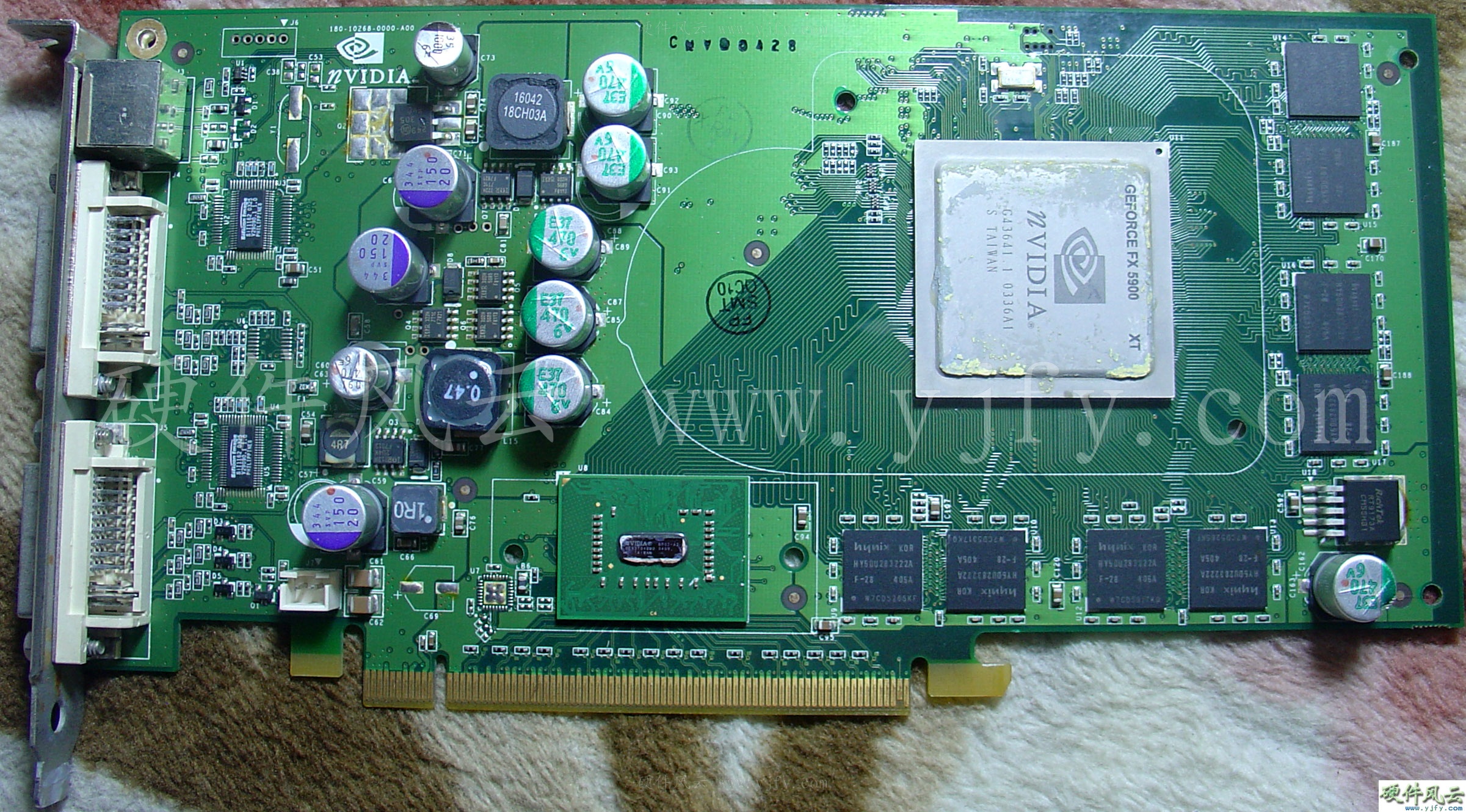
5.10 GeForce PCX5900
On February 17, 2004,
nVIDIA released GeForce PCX series graphics cards: GeForce PCX5950
(NV35), GeForce PCX5750 (NV36), GeForce PCX5300 (NV34) and GeForce
PCX4300 (GeForce4 MX 4000), which are essentially AGPs with bridge chip
BR02 Card.
5.10.1 P268 A00
Chip model:5900XT
PCB Code:180-10268-0000-A00
Chip date is 0336 weeks, PCB date is 0409 weeks.
GeForce PCX5900 Engineering sample
5.10.2 P268 A01
Chip model:5900XT
PCB Code:180-10268-0000-A01
Chip date is 0349 weeks, PCB date is 0421 weeks.
GeForce PCX5900
Engineering sample

nVIDIA later changed
the name of GeForce PCX5950 to Geforce PCX5900, but there are still
manufacturers using this form factor to make the so-called GeForce
PCX5950 graphics card.
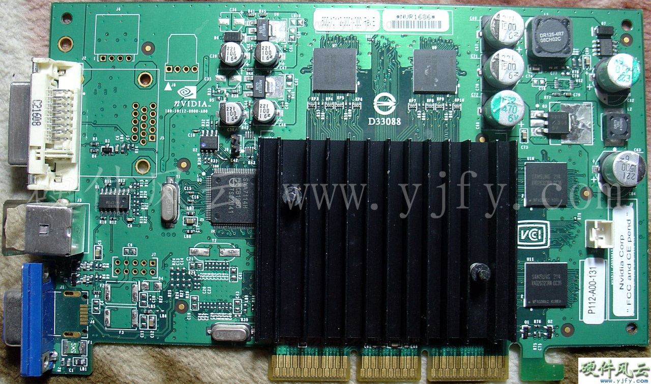
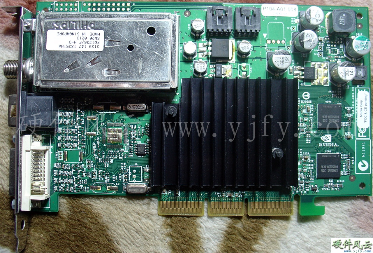
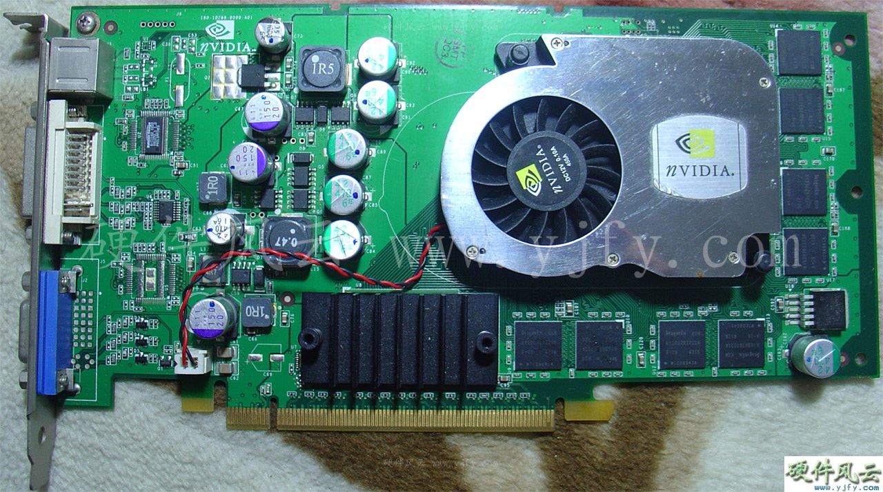
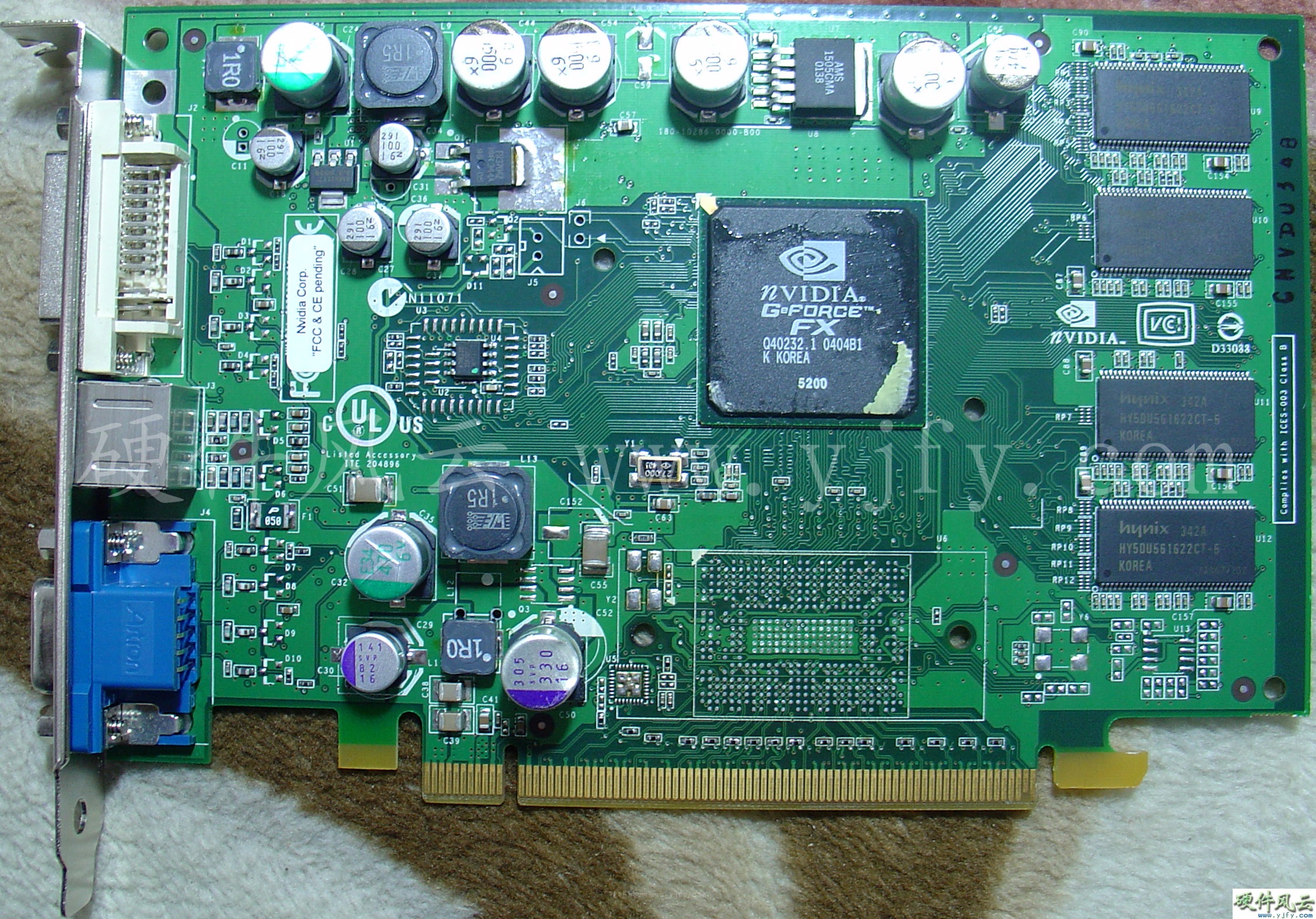
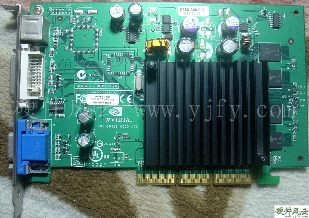
5.11 GeForce PCX5300
5.11.1 E286
Chip model:GF-FX-5200-B1
PCB Code:180-10286-0000-B00
Chip date 0404 week, PCB date 0407 week.
GeForce PCX5300 Engineering sample

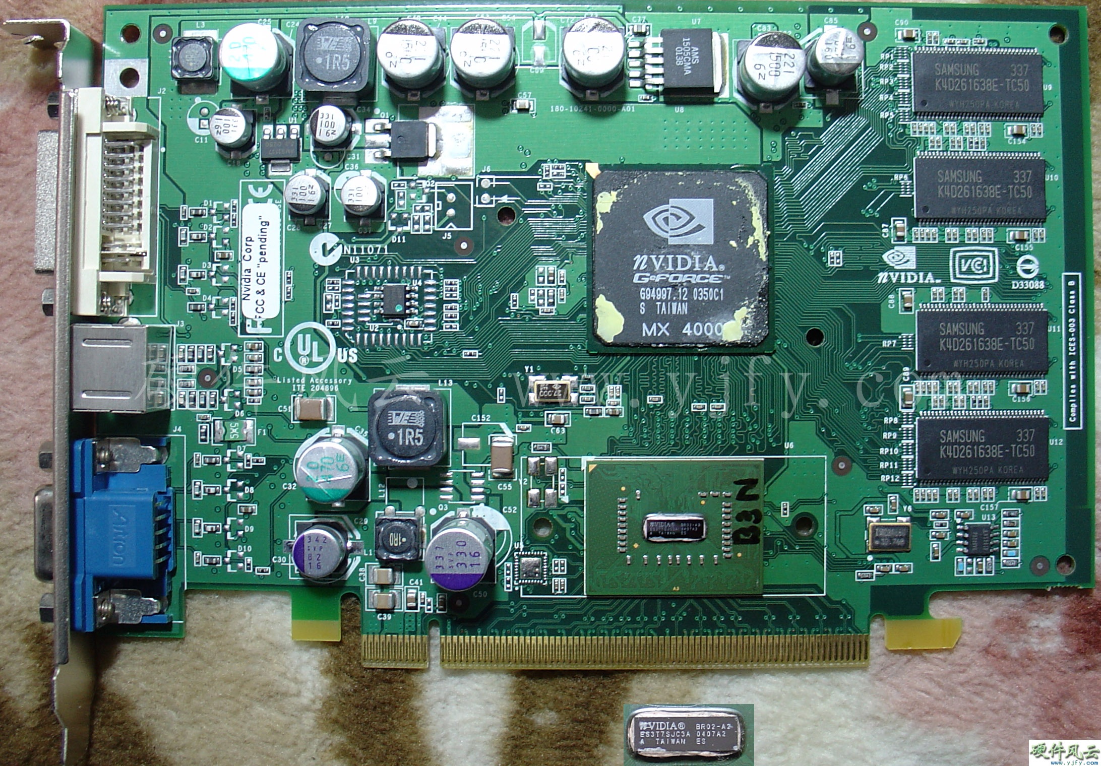
5.11.2 P241
Chip model:FX5200
B1S1 ES
PCB Code:180-10241-0000-A01
The chip date is 0344 weeks, and the PCB date is 0352
weeks. The BR02-A2 ES chip date is 0407 weeks.
GeForce PCX5300 Engineering sample

GeForce PCX 5750 (NV36) is a P269 form factor with a
similar appearance to the P241.
5.12 GeForce PCX5300
MCM
Used for mobile
devices and MXM interface graphics cards.
5.12.1 P233
PCB Code:180-10233-0000-B01
Chip model:NV37 A1 ES
Chip date is 0405 weeks, PCB date is 0405 weeks.
GeForce PCX5300 MCM Engineering sample
MCM (Multi-Chip
Module) is a packaging and packaging technology for bare dies, chips,
and integrated circuits. This packaging technology can encapsulate two
or more dies on one substrate. Usually, only one display core die is
packaged in the display chip. As mentioned earlier, nVIDIA GeForce4 Go
once packaged the display core and 2 or 4 video memories on a base to
save space and reduce energy consumption. It is mostly used on mobile
chips. Entering the PCI-E era, nVIDIA’s BR02 bridge chip is packaged on
the same base with the display chip and video memory through MCM
packaging.
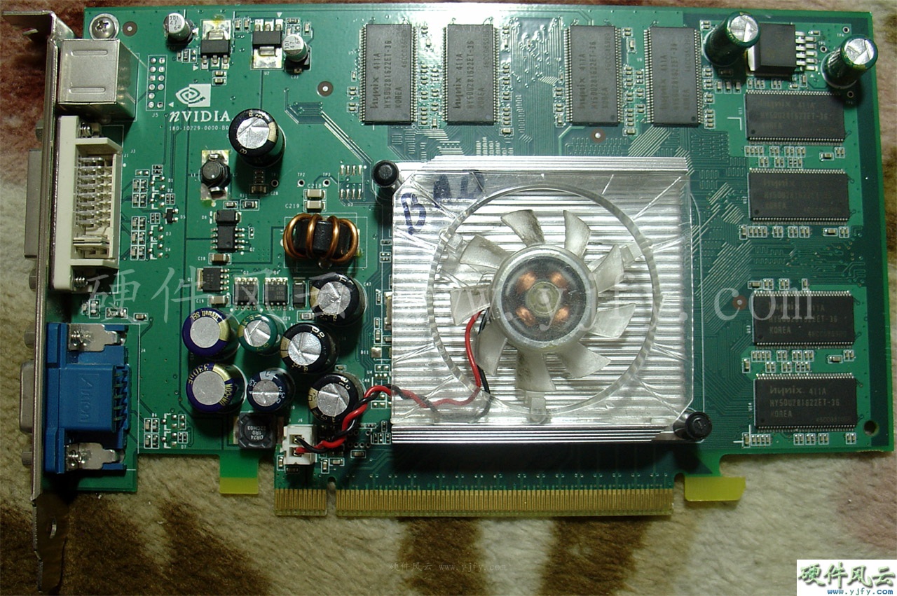
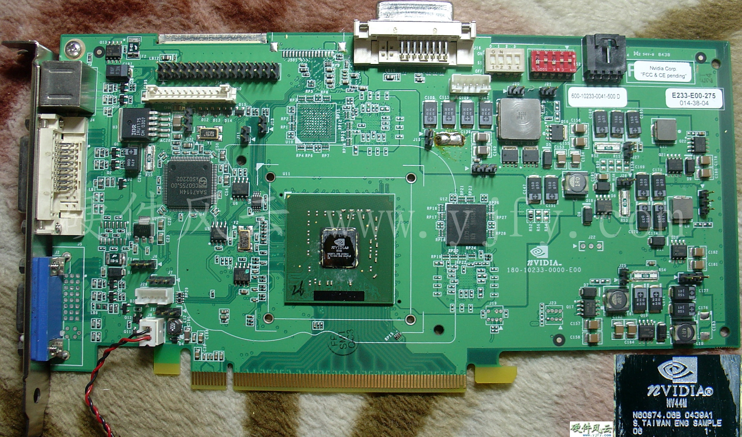
5.12.2 E233
PCB Code:180-10233-0000-A00
PCB date is 0352 weeks. The BR02 chip is packaged on
the same base as the graphics chip and video memory.
GeForce PCX5300 MCM Engineering sample

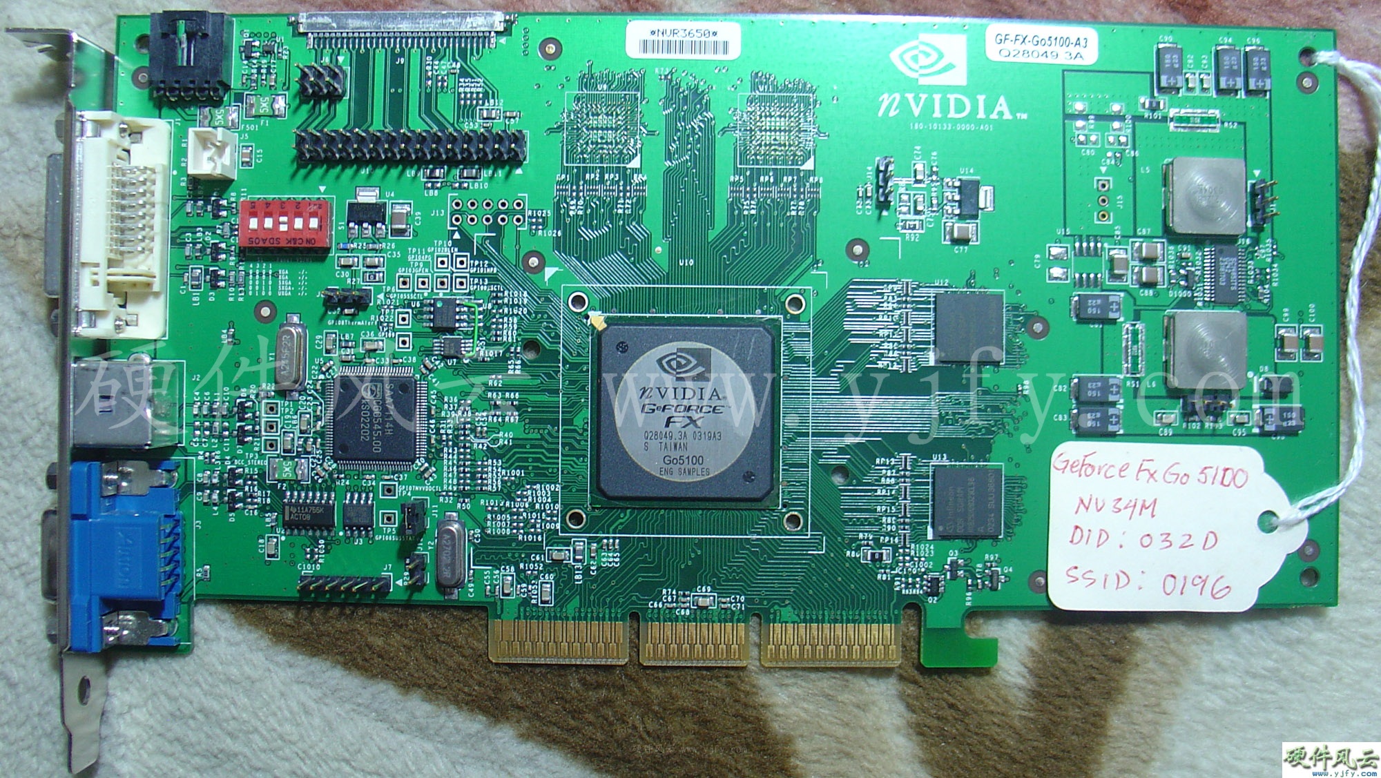
5.13 GeForce FX
Go5100
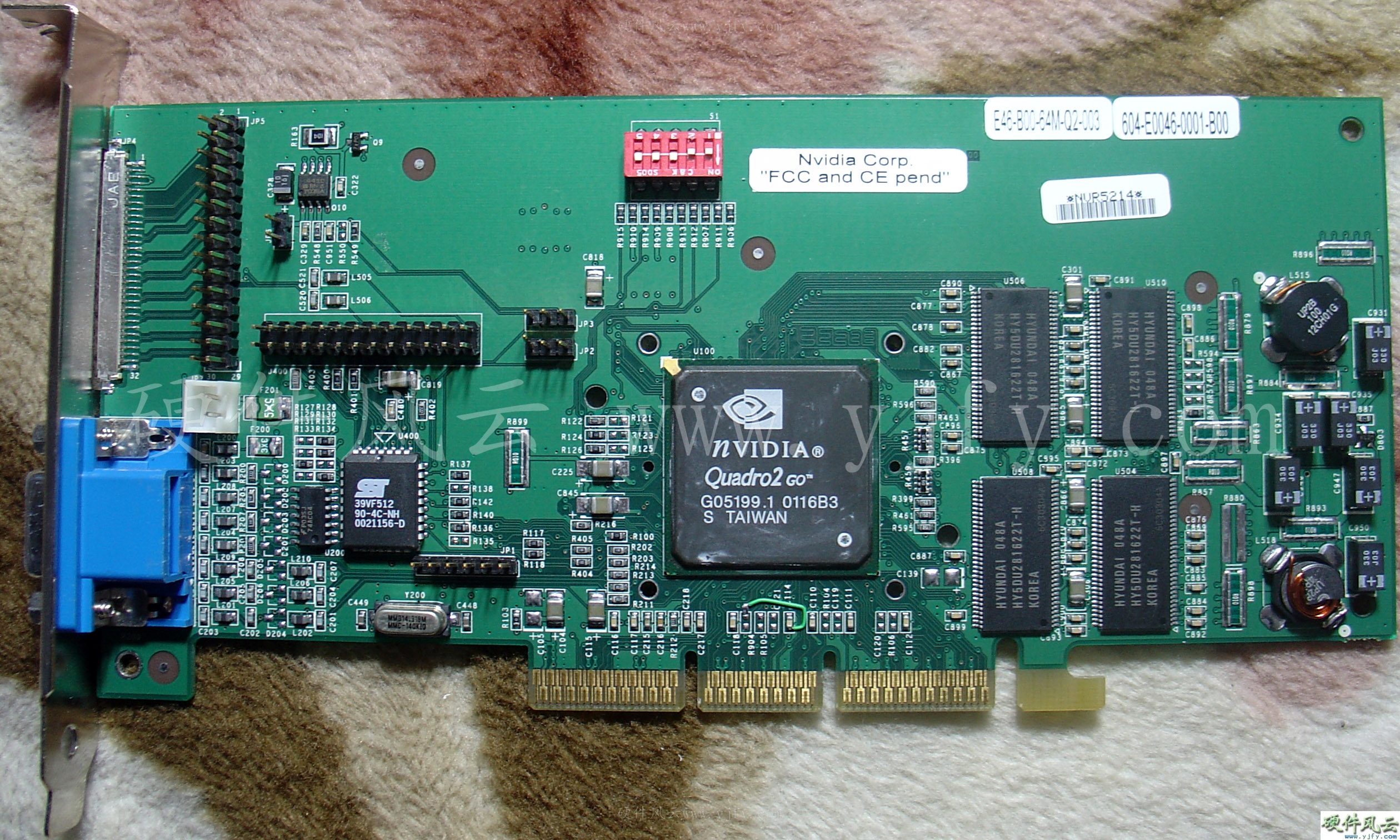
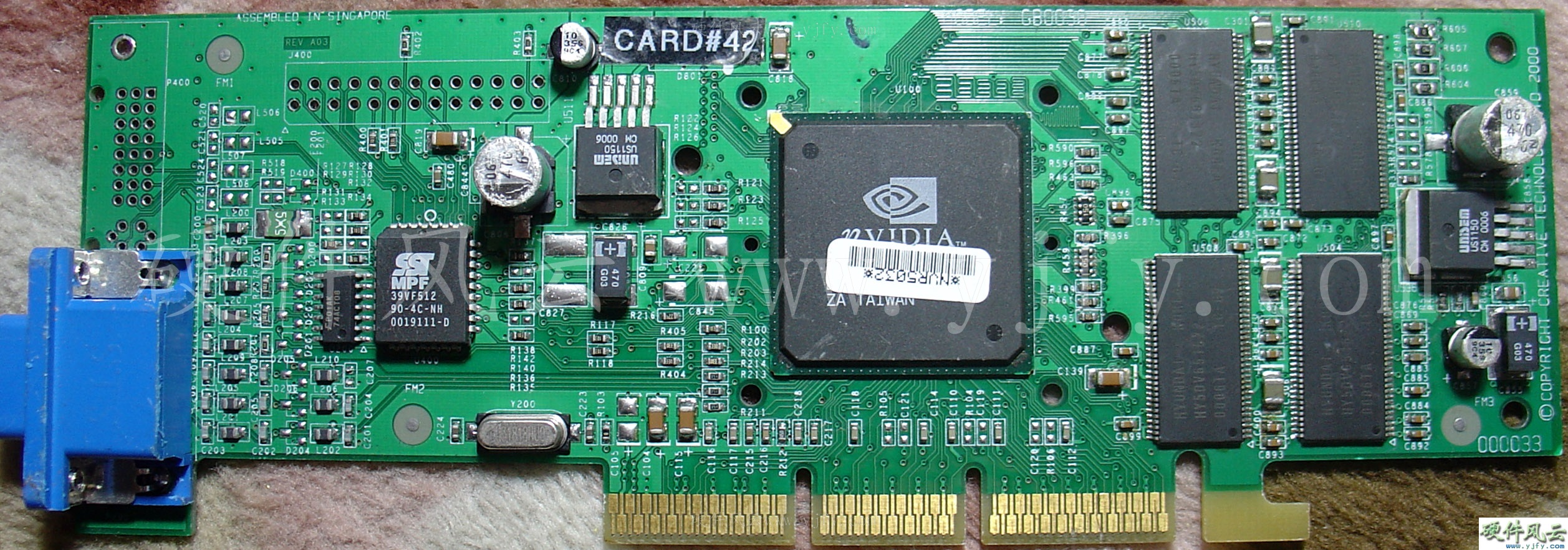
Model:E133
Chip model:Go5100
A3 ES
PCB Code:180-10133-0000-A01
Mobile Edition. Chip date is 0319 week, PCB date is
0317 week.
GeForce FX Go5100 Engineering sample
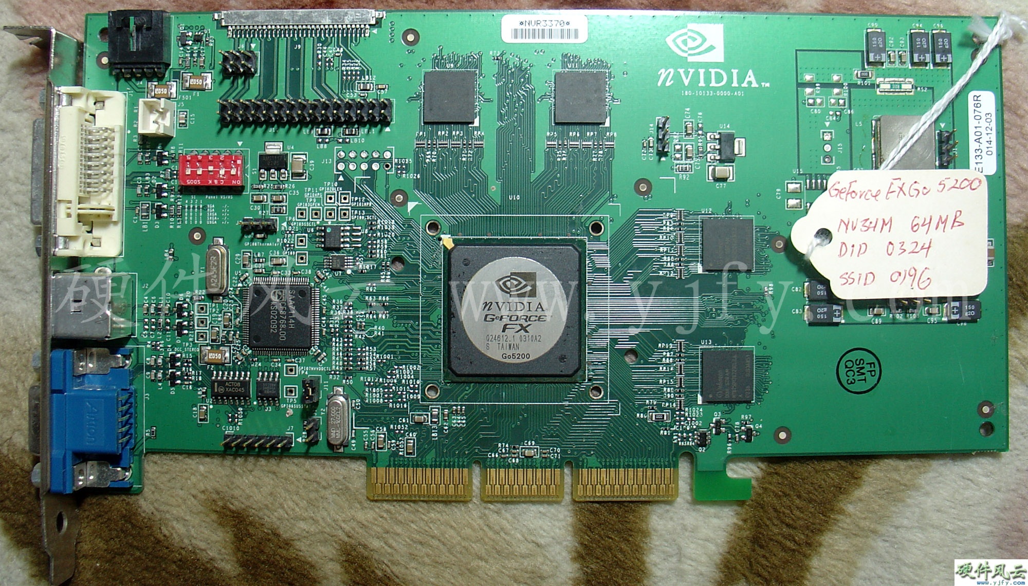
5.14 GeForce FX
Go5200
5.14.1 E133
Chip model:Go5200 A2
PCB Code:180-10133-0000-A01
Mobile Edition. Chip date is 0310 weeks, PCB date is
0305 weeks.
GeForce FX Go5200 Engineering sample
5.14.2 E134
Chip model:Go5200 A3
ES 64M
PCB Code:180-10134-0000-A02
Mobile Edition. Chip date is 0320 weeks, PCB date is
0319 weeks.
GeForce FX Go5200
MCM
Engineering sample
5.14.3 E15
PCB Code:180-10015-0000-A00
Chip model:MVP34 A2
ES 64MB
Mobile Edition. Chip date is 0309 weeks, PCB date is
0317 weeks.
GeForce FX Go5200
MCM
Engineering sample
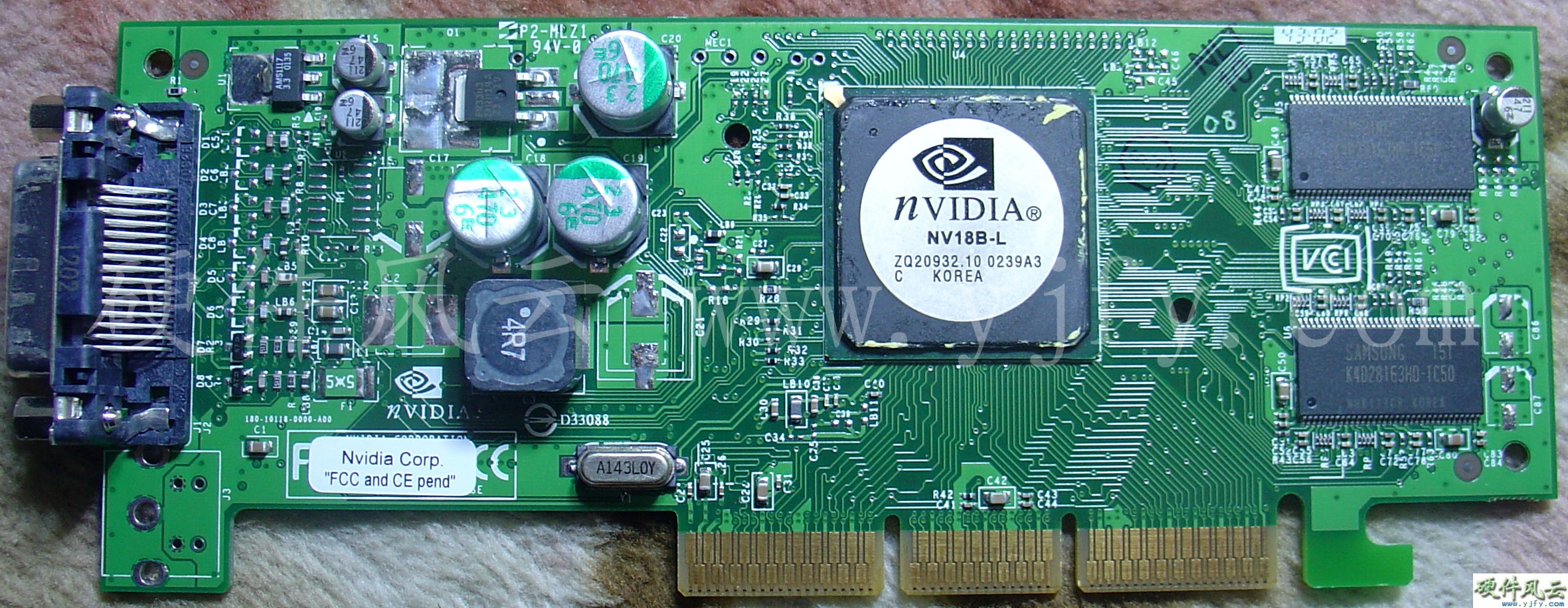
5.15 GeForce FX
Go5250
Model:E133
Chip model:Go5250 A3
PCB Code:180-10133-0000-A01
Mobile Edition. Chip date is 0327 weeks, PCB date is
0329 weeks.
GeForce FX Go5250 Engineering sample
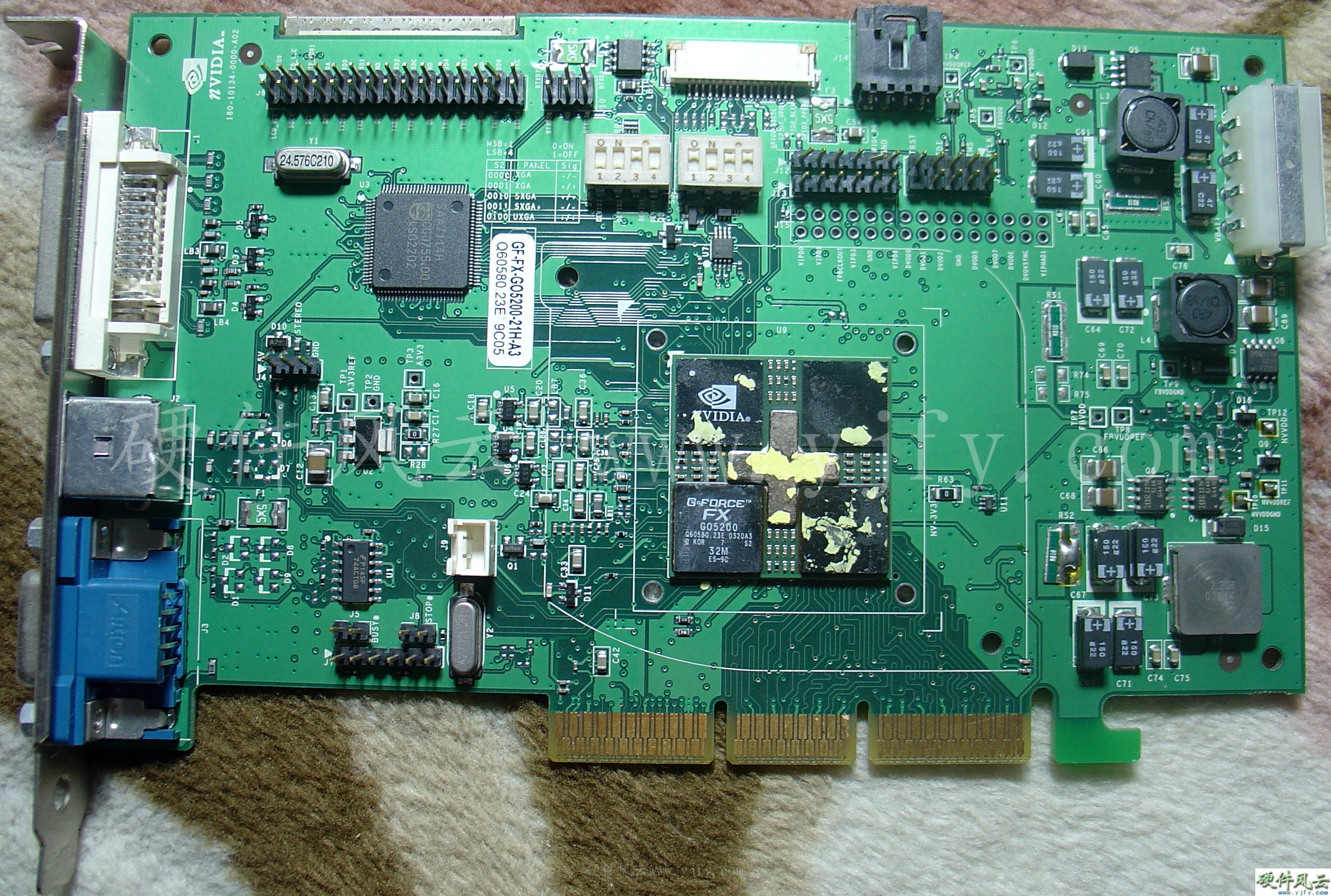
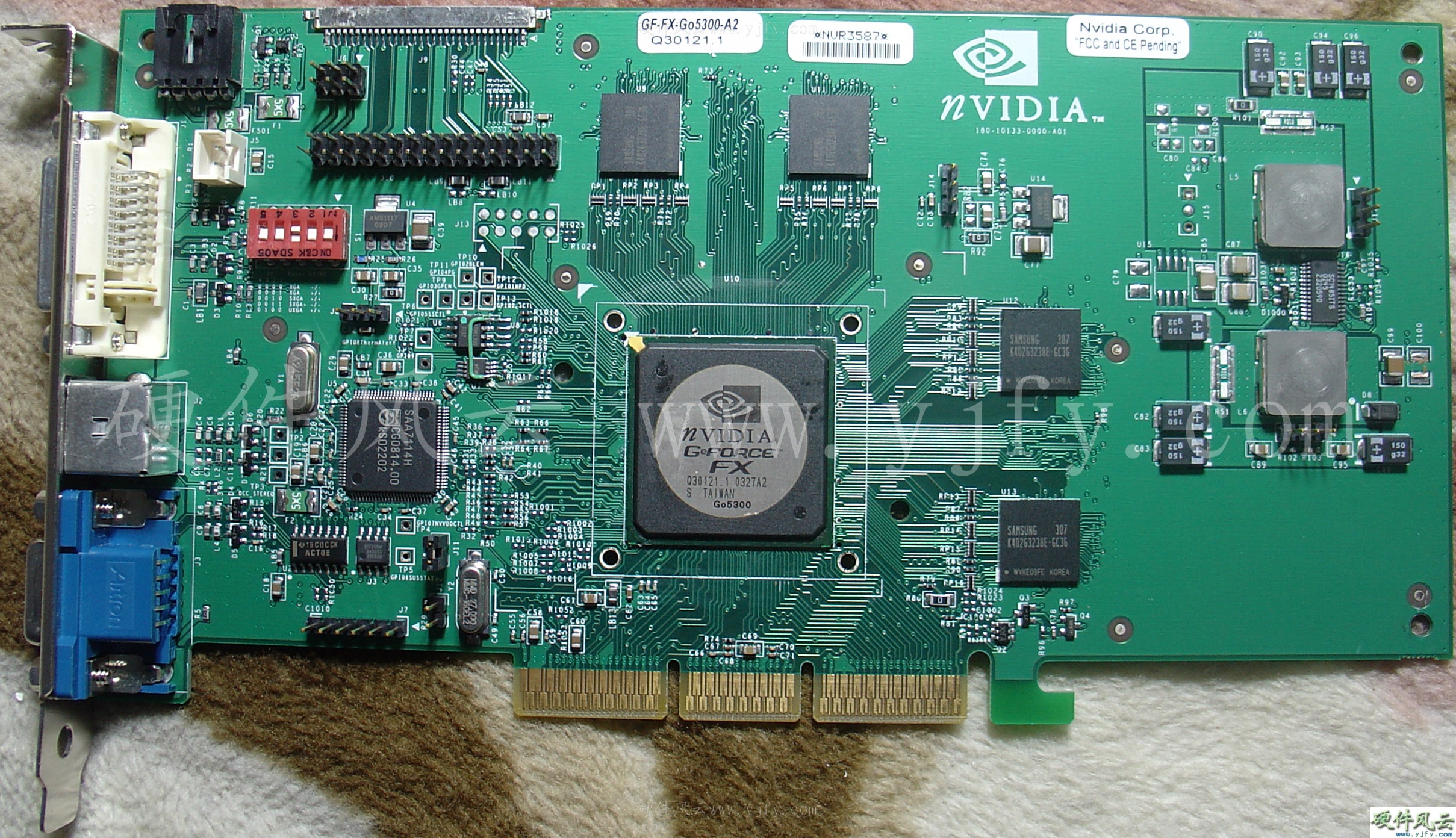
5.16 GeForce FX
Go5300
Model:E133
Chip model:Go5300 A2
PCB Code:180-10133-0000-A01
Mobile Edition. Chip date is 0327 weeks, PCB date is
0329 weeks.
GeForce FX Go5300 Engineering sample
5.17 GeForce FX
Go5600
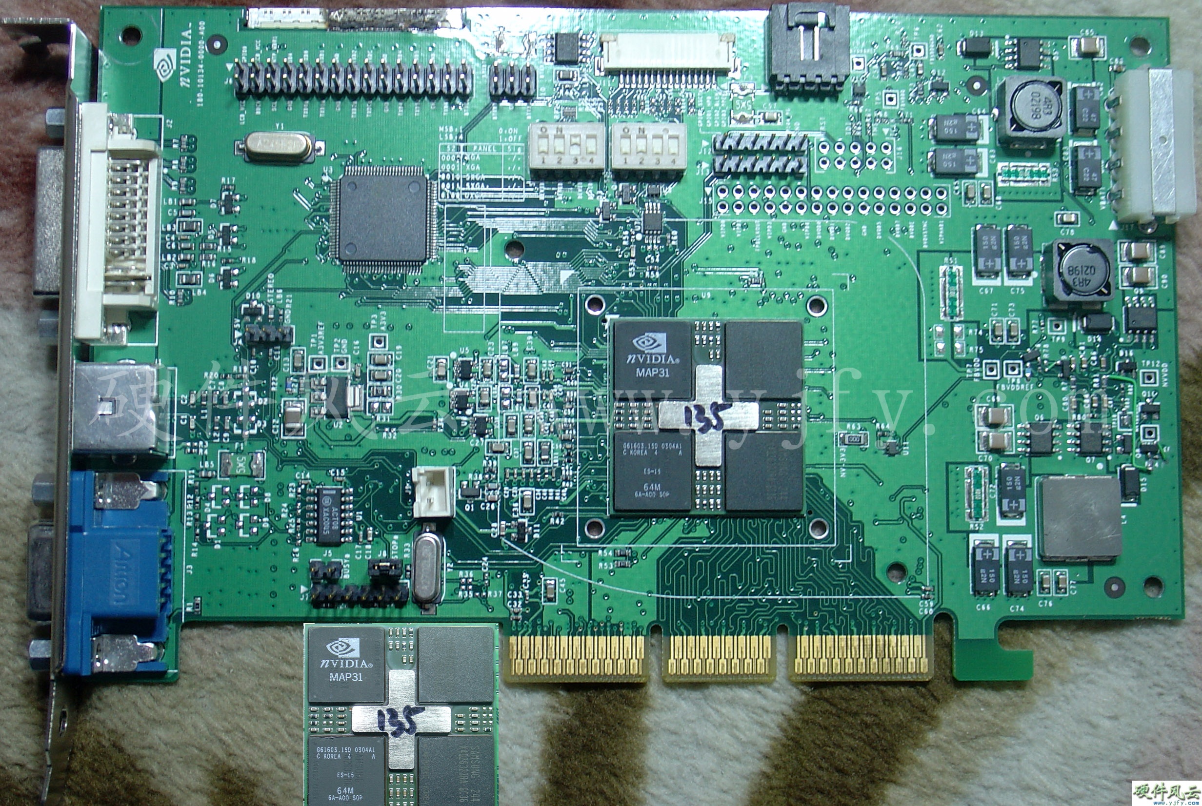
5.17.1 E133
PCB Code:180-10133-0000-A01
Chip model:Go5600 A1
Mobile Edition. Chip date is 0338 weeks, PCB date is
0308 weeks.
GeForce FX Go5600 Engineering sample
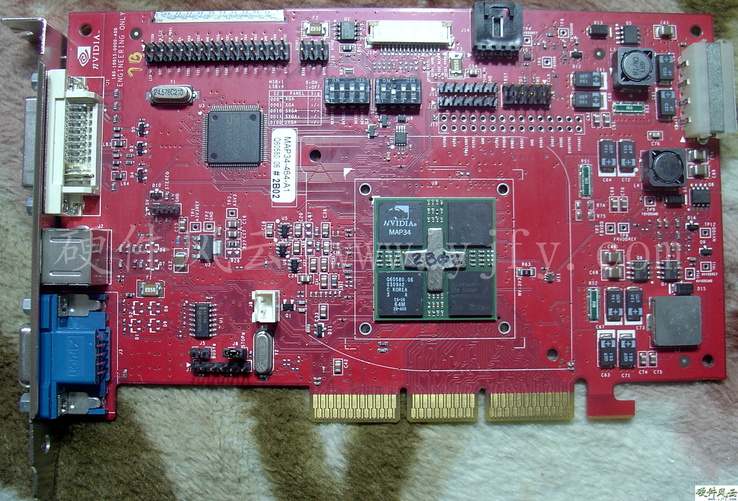
GeForce FX Go5600
MCM
5.17.2 E134
PCB Code:180-10134-0000-A00
Chip model:MAP31
A1 ES
Mobile Edition. The chip date is 0304 weeks, and the
PCB date is 0251 weeks.
GeForce FX Go5600 MCM Engineering sample
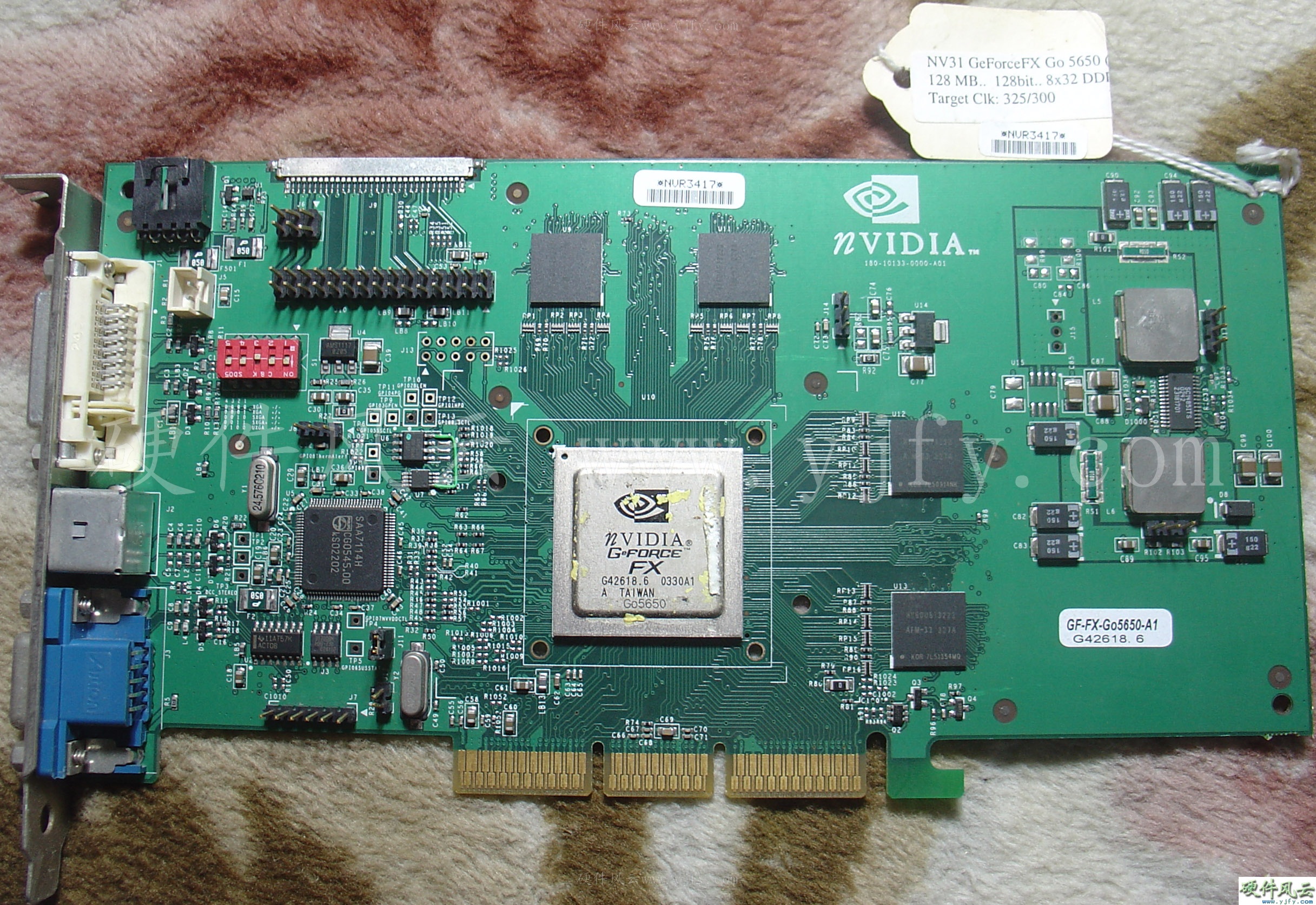
5.18 GeForce FX
Go5650
Model:E133
Chip model:Go5650 A1
PCB Code:180-10133-0000-A01
Mobile Edition. Chip date is 0330 weeks, PCB date is
0315 weeks.
GeForce FX Go5650
Engineering sample
5.19 GeForce FX
Go5700
5.19.1 E183
Chip model:NV36M
A1 ES
PCB Code:180-10183-0000-A01
Mobile Edition. Chip date is 0344 weeks, PCB date is
0344 weeks.
GeForce FX Go5700
Engineering sample
5.19.2 P183
Chip model:GF-FX-Go5700
A1
PCB Code:180-10183-0000-A01
Mobile Edition. Chip date is 0346 weeks, PCB date is
0350 weeks.
GeForce FX Go5700
Engineering sample
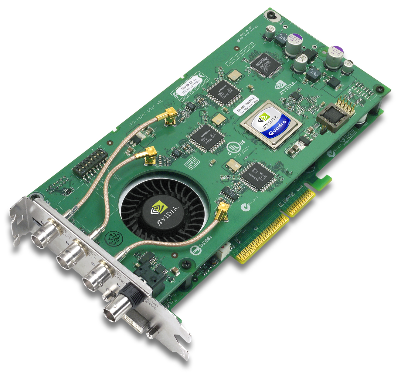
5.20 Quadro FX1000
Model:P126
PCB Code:180-10126-0000-A04
Chip model:NV30GL A1
Released on January 21, 2003. The chip date is 0244
weeks, and the PCB date is 0249 weeks.The official version of Quadro
FX1000 adopts the P128 form factor of Quadro FX2000.
Quadro FX1000
Engineering sample
5.21 Quadro FX2000
Model:P128
PCB Code:180-10128-0000-A00
Chip model:FX2000-A2X-ES
Released on January 21, 2003. The chip date is 0252
weeks, and the PCB date is 0301 weeks.
The official version of Quadro FX2000 does not use
GeForce FX5800
Ultra's cooling system.
Quadro FX2000
Engineering sample
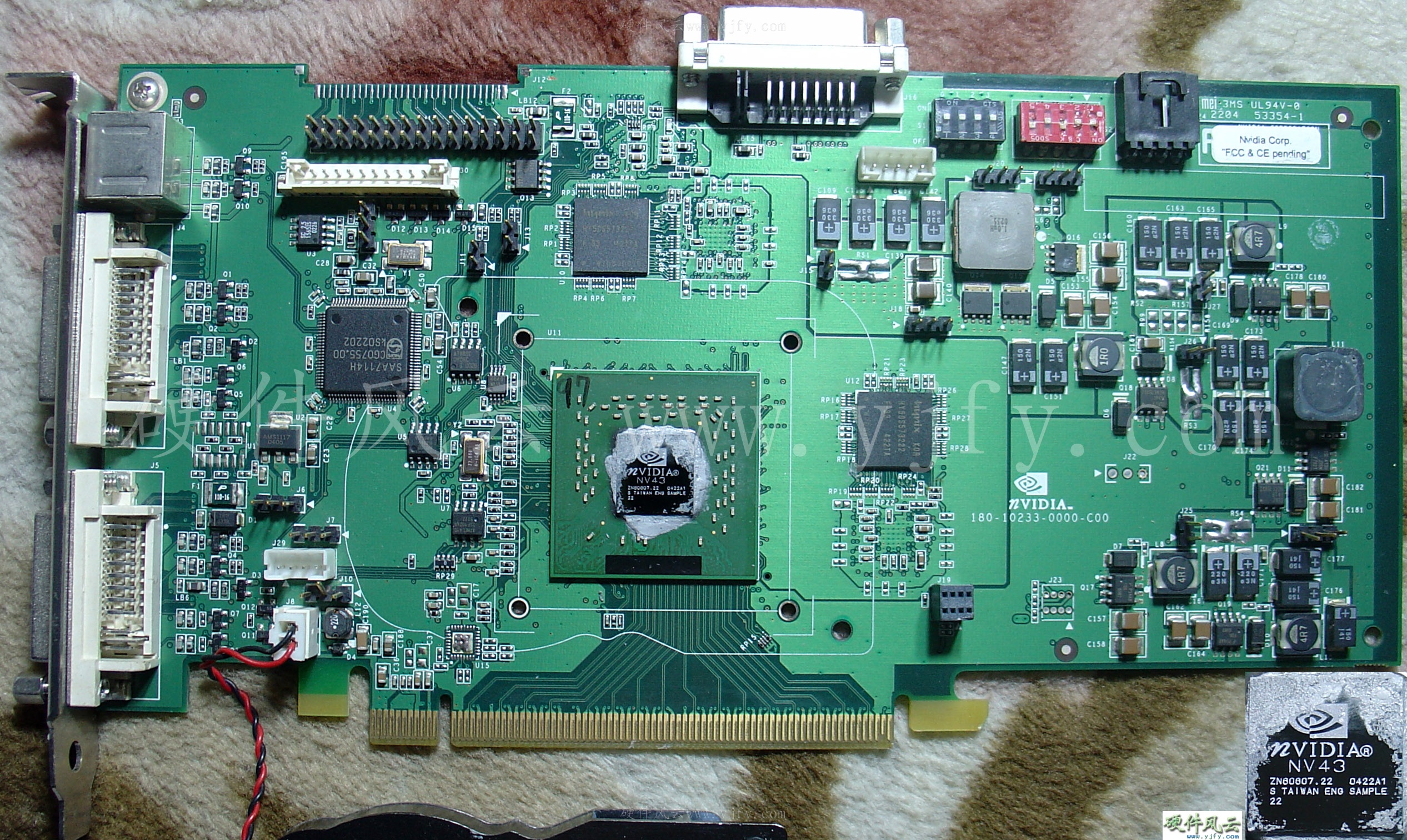
5.22 Quadro FX3000
Released on July 22, 2003.
5.22.1 P170-B01
Chip model:NV35GL
A1S2 ES
PCB Code:180-10170-0000-B01
Chip date is 0314 weeks, PCB date is 0314 weeks.
Quadro FX3000 Engineering sample
5.22.2 E174-A00
PCB Code:180-10174-0000-A00
Chip model:FX3000 A1
Chip date is 0319 weeks, PCB date is 0321 weeks.
Evaluation board, not disassembled, the chip should be ES.
Quadro FX3000 Engineering sample
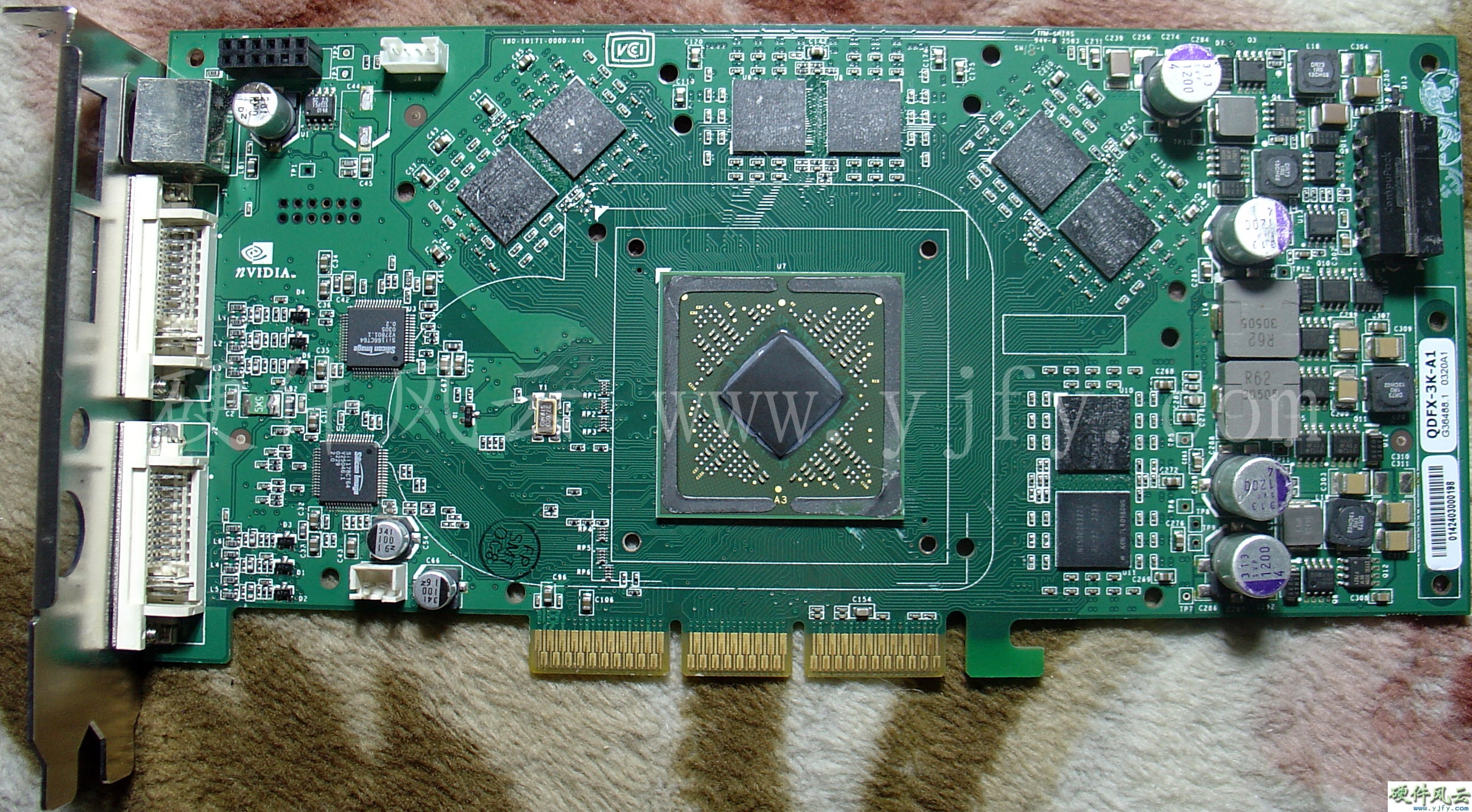
5.22.3 P171-B00
PCB Code:180-10171-0000-B00
Chip model:FX3000 A1
Chip date is 0333 weeks, PCB date is 0334 weeks.
Quadro FX3000 Engineering sample
5.22.4 P171-A01
Chip model:Quadro
FX3000 A1
PCB Code:180-10171-0000-A01
Chip date is 0320 weeks, PCB date
is 0325 weeks.This board type Quadro FX3000 graphics card adds P154
daughter card (support Framelock and Genlock function) is Quadro
FX3000G.
Quadro FX3000 Engineering sample

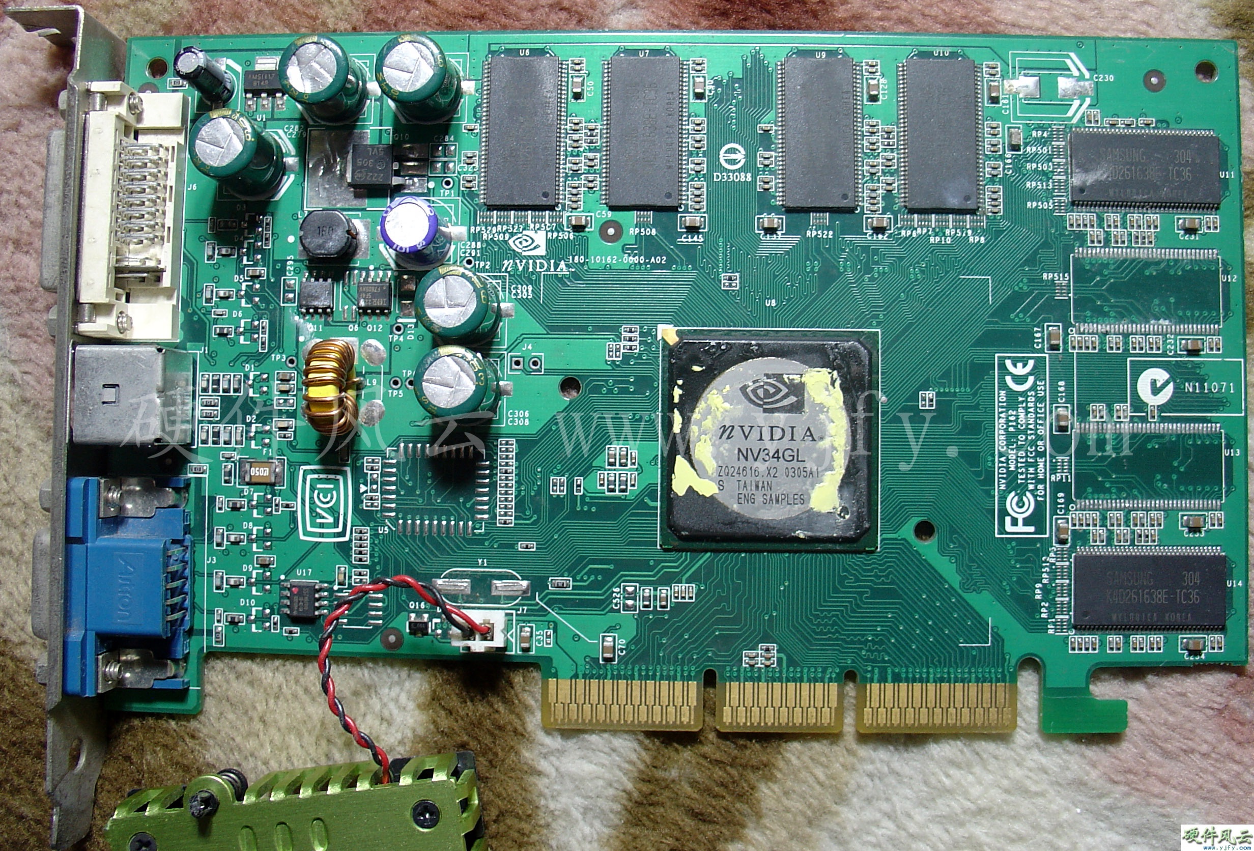
5.23 Quadro FX500
Released on May 21, 2003.
5.23.1 P162
Chip model:NV34GL A1
ES
PCB Code:180-10162-0000-A02
Chip date is 0305 weeks, PCB date is 0307 weeks.
Quadro FX500 Engineering sample
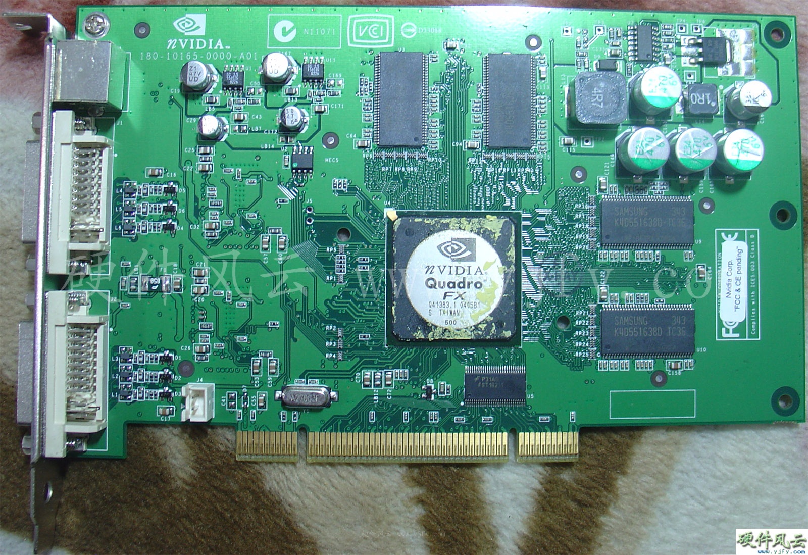
5.23.2 P165
Chip model:QUADRO FX
500 B1
PCB Code:180-10165-0000-A01
Chip date is 0405 weeks, PCB date is 0407 weeks.
Quadro FX500 Engineering sample

5.24 Quadro FX700
Released on March 17, 2004.
5.24.1 E133
PCB Code:180-10133-0000-A00
Chip model:NV31GL_A1+
The chip date is 0302 weeks, and the PCB date is 0252
weeks.
Quadro FX700 Engineering sample

5.24.2 P141
Chip model:NV31GL A1+
PCB Code:
Prototype cards without PCB Code are very rare and may be
180-10141-0000-A01.
Chip date is 0302 weeks, PCB date is 0250 weeks.
Quadro FX700 Engineering sample
There are also Quadro
FX1100 (NV36GL) using P192 form factor, Quadro FX1300 (NV36GL) using
P268 (GeForce PCX 5900/5950) form factor, and nVIDIA NVS 280 (NV34).
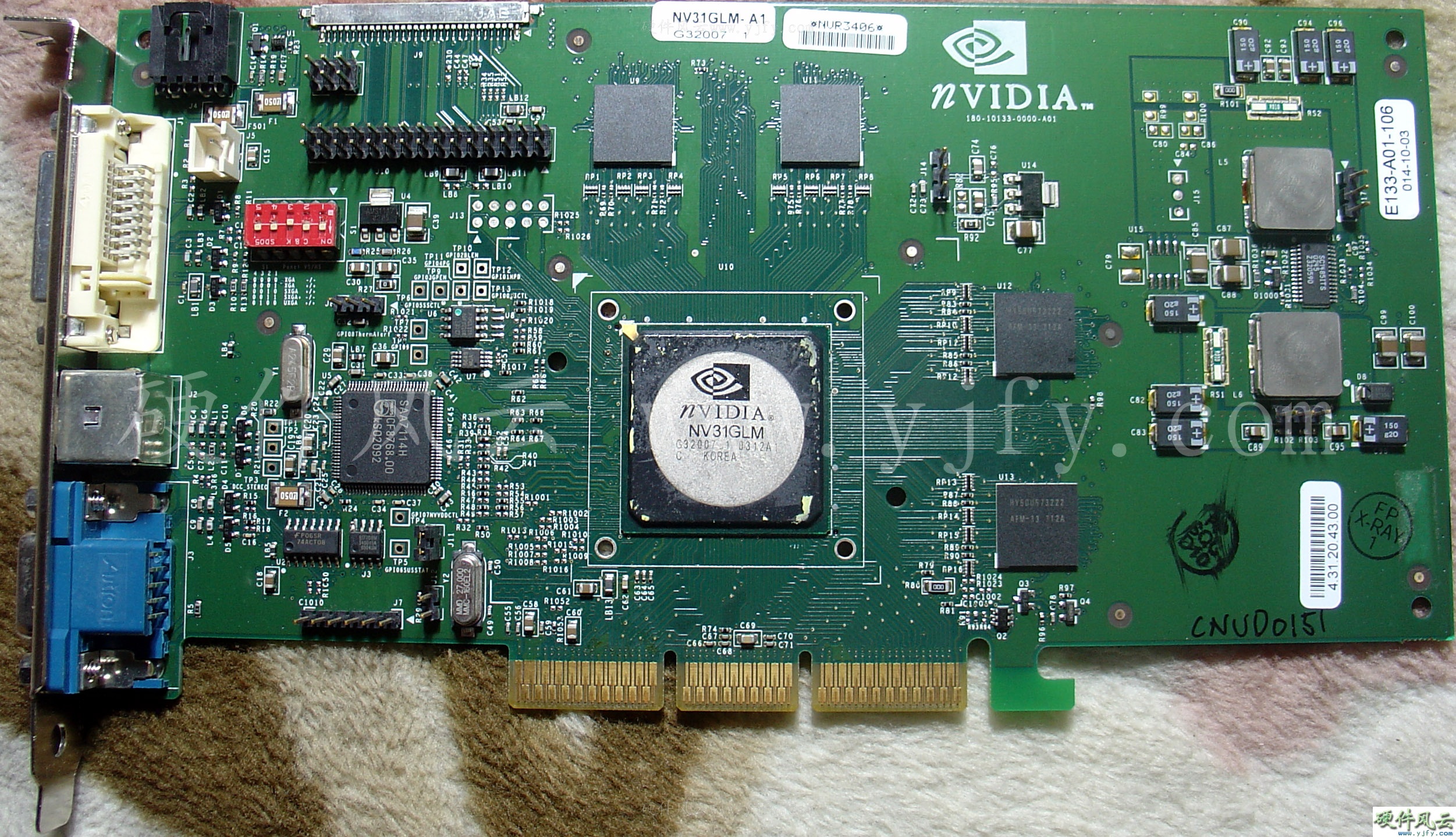
5.25 Quadro FX Go700
Model:E133
Chip model:NV31GLM A1
PCB Code:180-10133-0000-A01
Released on June 25, 2003. Mobile version, chip date
is 0312 weeks, PCB date is 0313 weeks.
Quadro FX Go700 Engineering sample

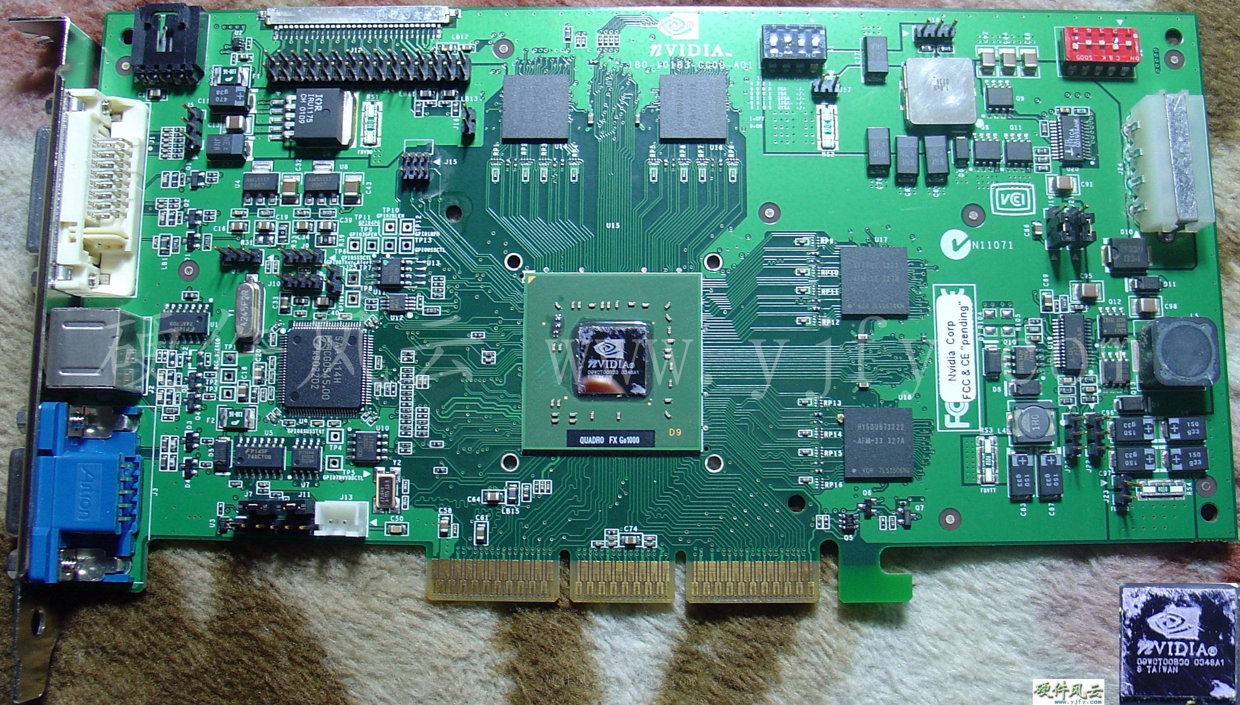
5.26 Quadro FX
Go1000
Model:E183
PCB Code:180-10183-0000-A01
Chip model:Go1000 A1
Released on February 25, 2004. Mobile version, chip
date 0348 weeks, PCB date 0350 weeks.
Quadro FX Go1000 Engineering sample

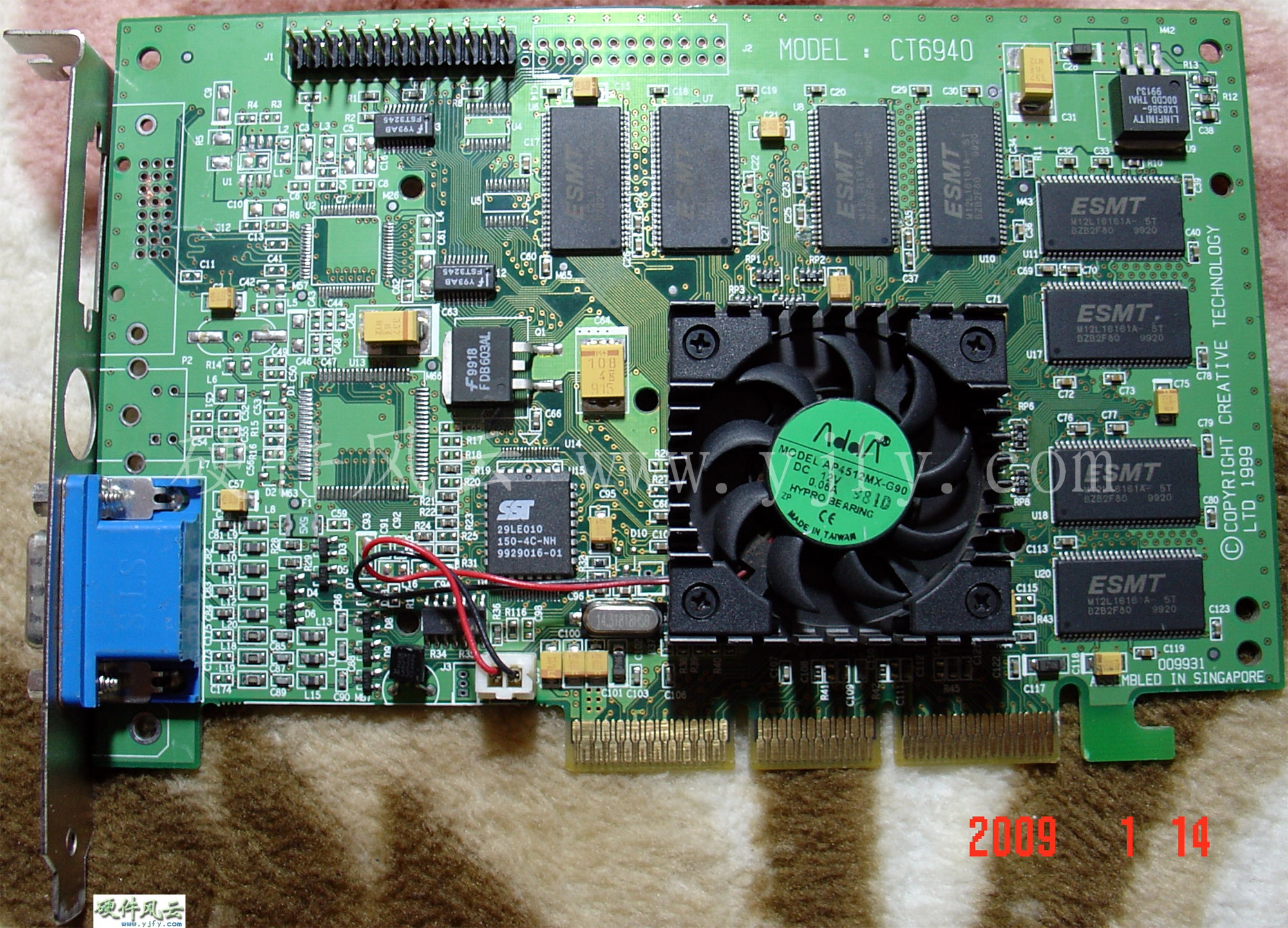
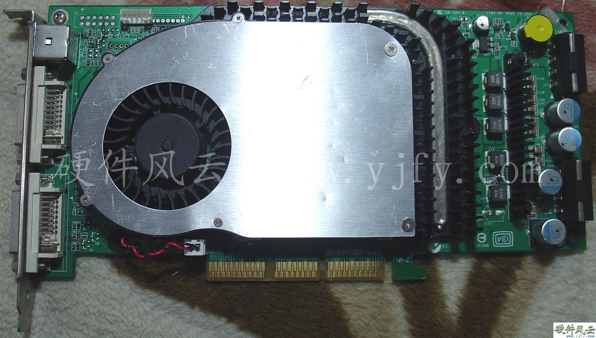
5.27 Abit
The Siluro GeForce FX 5800 prototype card uses
nVIDIA's T01 prototype card to promote the new product and uses the "OTES
III" cooling system.
Siluro GeForce FX
5800 Engineering sample

(From
computerbase.de)
|


